PCB Board Assembly Work: A Comprehensive Overview
Introduction
Assembling PCBs is a task that requires a high level of technical expertise, involving multiple precise processes. From interpreting design schematics to actual layout, drilling, copper plating, component placement, and soldering, each step requires meticulous control to ensure the correct placement and connection of components. Furthermore, as electronic devices progress toward smaller scales and higher efficiency, the PCB board assembly work process has become increasingly complex. In the electronics manufacturing industry, PCB assembly is considered a fundamental and critical step. With continuous technological advancements, this workflow is constantly being optimized and innovated to better meet the growing market demands. A deep understanding of the PCB board assembly work process is crucial for electronic engineers and manufacturers to enhance product quality and increase market competitiveness.
Preparation Before PCB board assembly work
Careful Material Selection: Laying a Solid Foundation for Quality
In the PCB assembly process, material selection is crucial as it determines the performance and durability of the circuit board. Various PCB materials are available on the market, including but not limited to FR-4 and high-frequency laminates, each with its unique applications and characteristics. Proper material selection helps ensure circuit stability and lossless signal transmission. Additionally, surface treatment technologies such as HASL or ENIG are equally important for improving soldering quality, enhancing corrosion resistance, and ensuring long-term durability.
Detailed Design Review: Refining the Layout
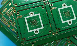
The design phase of the PCB layout is an indispensable part of the assembly process. A well-thought-out layout design can effectively reduce potential issues during subsequent assembly stages. Key points in the design review include rational component placement to avoid electromagnetic interference and hotspots while ensuring simplified routing to reduce resistance and improve signal transmission efficiency. The design review should also consider practical assembly processes to ensure that the design schematics perfectly align with the actual assembly workflow.
Basic Workflow of PCB Assembly
Drilling operation
Drilling plays a crucial role in the PCB manufacturing journey. It is not merely about creating simple holes in the laminate but providing physical pathways for various electronic components, thus establishing the basic functionality of the circuit board. Precise drilling technology ensures accurate component placement and reliable circuit connections, which is key to a smooth assembly process.
Plating through hole technology
Next is the sophisticated application of through-hole plating technology. This process involves applying a layer of conductive material to the hole walls, enhancing the connectivity of the PCB, and bridging the internal and external layers. This technology significantly increases the complexity and functionality of the circuit board, which is essential for maintaining stable connections between electronic components.
SMT (Surface Mount Technology) and through-hole insertion
Following this, we arrive at the detailed operations of SMT (Surface Mount Technology) and through-hole insertion. SMT is known for its ability to precisely place small components on the PCB surface, while through-hole insertion is more suitable for larger or specially mounted components. These two technologies complement each other, ensuring high-density assembly requirements and stable component fixation.
Soldering
Soldering is the climax of the PCB assembly process. Wave soldering is favored for its suitability for through-hole components, creating strong electrical and mechanical connections by melting solder. Reflow soldering, on the other hand, focuses on SMT components, using precise temperature control to melt and solidify solder, completing the tight bonding of components and the circuit board.
The entire PCB assembly process is a collection of precise processes. From accurate drilling to decisive soldering, each step is a rigorous test of the final product’s quality and performance. Mastering these basic processes is key to improving electronic product reliability and enhancing market competitiveness.
Quality Management in PCB Assembly
Quality Control: The Guardian of the Assembly Process
In the world of electronic assembly, quality control is the guardian of product reliability and performance. It is a continuous thread from raw material inspection to final product testing, with each stage requiring strict quality monitoring. Its role is not only to prevent potential defects but also to identify and correct issues before they occur, thus avoiding costly rework and product recalls.
Common Issues and Solutions: Prevention and Mitigation
In PCB assembly, various common issues may arise, and preventing and solving these issues requires a systematic quality management approach. For instance, soldering defects can be prevented by adjusting soldering parameters and improving operator skills; component misalignment can be avoided through precise machine calibration and rigorous visual inspections; while short circuits require detailed design reviews and material selection to prevent.
The quality of PCB assembly directly reflects the performance and lifespan of electronic products. Establishing a rigorous quality control system can effectively prevent and address various issues that arise during assembly, enhancing the product’s market competitiveness and earning consumer trust and a good reputation for the company. Through this, quality control becomes a bridge connecting products and the market, ensuring the continuous advancement of the electronics industry.
Post-Assembly Testing and Inspection
Functional Testing: Ensuring Design Intent is Achieved
Completing PCB assembly is just the beginning; functional testing is key to ensuring that the product meets design intentions. This phase involves comprehensive testing under simulated operational conditions, including signal integrity, power stability, and interface response speed. Such testing confirms that the PCB operates reliably in expected environments, serving as a strong guarantee of product performance and reliability.
Visual Inspection: The Sharp Eye for Defect Detection
Additionally, visual inspection plays a crucial role in quality control as the first line of defect detection. Whether through meticulous manual observation or automated visual inspection technology, this process uncovers any soldering flaws, component placement errors, or circuit shorting and disconnections. The precision of visual inspection not only highlights issues but also provides opportunities for rapid adjustments to the production process.
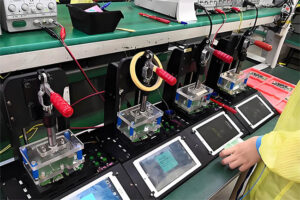
The quality of PCB assembly is the foundation of electronic product performance and safety. Functional testing and visual inspection, as the two key stages post-assembly, provide dual assurances for high-quality circuit boards. This series of detailed testing and inspection helps capture and resolve potential issues promptly, serving as a crucial means to enhance product quality and market competitiveness.
Modern Technologies in PCB Assembly
Automation: A Leap in Efficiency and Accuracy
The pace of technological innovation has never slowed, playing a revolutionary role in the PCB assembly industry. The significance of automation technology is increasingly evident, not only greatly improving production efficiency but also reducing human error through precise mechanical operations, ensuring consistency in the assembly process and high standards of product quality. Automation technology, from automatic pick-and-place machines to robotic soldering systems, has made PCB assembly more precise and efficient.
3D Printing Technology: An Innovative Assembly Process
3D printing technology showcases immense potential in PCB assembly. This technology can quickly create complex circuit board structures and has the potential to enable integrated printing of electronic components. It significantly shortens the product’s time from concept design to market launch and opens doors for personalized and small-batch production. The application of 3D printing technology signifies that PCB assembly processes are evolving towards greater flexibility and innovation.
With the application of modern technologies like automation and 3D printing, the PCB assembly work is undergoing a technological revolution. Automation technology enhances production efficiency and product quality, while 3D printing brings new possibilities to the assembly process. These technological advancements not only accelerate the development of the PCB assembly industry but also lay a solid foundation for innovation in electronic products.
Future Trends in PCB Assembly
Miniaturization and Integration: Reaching New Heights in Precision and Density
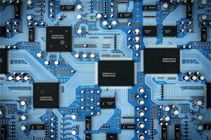
As electronic devices increasingly pursue smaller sizes and richer functionality, PCB assembly processes face a revolution in precision and density. The trend towards miniaturization demands clever placement of more functional components in a compressed space, challenging assembly technology’s precision and setting higher standards for circuit stability and reliability. Meanwhile, the development of integration has given rise to multi-layer boards and three-dimensional assembly technologies, which expand circuit design complexity in the vertical dimension, enhancing electronic device performance.
Green Manufacturing: The Rise of Eco-Friendly Materials
The use of eco-friendly materials marks the PCB assembly industry’s move towards a greener future. With global emphasis on environmental protection, finding and adopting recyclable and low-toxicity materials has become a new industry challenge. Applying these eco-friendly materials not only helps reduce the environmental impact of electronic waste but also actively responds to increasingly stringent environmental regulations. From eco-friendly solder to biodegradable substrate materials, the widespread use of green materials is gradually shaping a new image for the PCB assembly industry.
Future Outlook: Harmonious Progress in Miniaturization, Integration, and Sustainability
The PCB assembly industry stands on the threshold of a new era, evolving towards greater miniaturization, integration, and environmental sustainability. These trends represent new directions in technological advancement and the dual pursuit of electronic product quality and environmental responsibility. As these trends continue to develop, PCB assembly work will remain at the forefront of the electronics manufacturing industry, leading the sector toward a more efficient and eco-friendly future.
Conclusion
PCB board assembly work is a comprehensive engineering process involving multiple disciplines and technologies. With the rapid development of the electronics industry, this field continues to innovate and progress. From design to testing, each stage has a decisive impact on the final product’s performance. A thorough understanding of the PCB board assembly work is crucial for improving product quality, reducing costs, and accelerating time-to-market.




Leave A Comment