The Art of Electronic Circuit Board Assembly
Introduction
Driven by the wave of digitalization, electronic devices dot our everyday lives like stars in the sky. Whether small like smartphones or large like servers in data centers, they all share a common foundation—the printed circuit board (PCB). These inconspicuous little boards carry complex electronic networks and are an indispensable part of modern technology. This article takes readers on a deep dive into the art of PCB assembly, uncovering the stories of craftsmen who create technological miracles in the microscopic world.
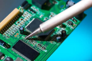
The Secrets of PCB Assembly
Basics and Functionality
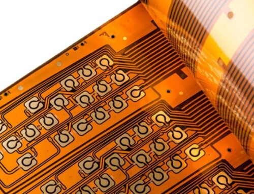
PCBs typically consist of an insulating substrate, conductive tracks (traces), and various electronic components mounted on the board. Their core function is to provide electrical connections for electronic components, allowing current to flow along predefined paths and execute specific electronic functions.
Assembly Process
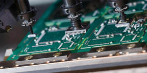
The assembly process usually begins with the design phase, where designers use specialized software to create circuit diagrams. These diagrams are then transferred onto the substrate using automated or semi-automated machines, forming the conductive traces. Next comes component placement and soldering. This process requires extreme precision and attention to detail.
The Importance of Precision
In PCB assembly, even the smallest deviation can lead to the failure of the entire circuit. Precision is the lifeblood of this work. Every solder joint and every trace must meet design specifications to ensure the stability and reliability of the circuit.
The Craftsman’s Skill
The Blend of Handwork and Machinery
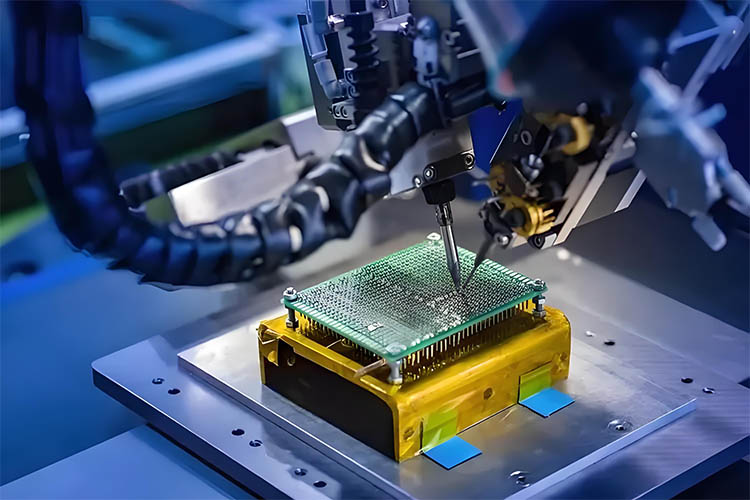
In PCB assembly, the craftsman’s skill is reflected in the delicate mastery of manual operations and the proficient use of machinery. Hand soldering is crucial for installing precision components, requiring craftsmen to have steady and accurate movements.
Continuous Learning and Adaptation
With the rapid development of electronic technology, new components and assembly techniques are constantly emerging. Craftsmen must continually learn and master advanced assembly methods, such as Surface Mount Technology (SMT), to adapt to industry changes.
Innovation and Challenges
The Trend of Miniaturization
As electronic devices become smaller, lighter, and more efficient, PCB miniaturization has become a significant trend. This requires assembly techniques to accommodate smaller components and tighter layouts.
Environmental Requirements
Environmental regulations have imposed stricter requirements on PCB assembly. Lead-free soldering and the use of eco-friendly materials have become industry standards, posing technical challenges and new demands on craftsmen’s skills.
Lead-Free Soldering Process Standards
The primary standards for lead-free soldering processes include:
IPC-7095C Lead-Free Printed Circuit Board Industry Standard
J-STD-020C Challenges for Lead-Free Implementation
IPC-TM-650 Standard Test Methods
IPC-A610E Lead-Free Printed Circuit Board Acceptance Standard
These standards outline the requirements for the design, selection, validation, and verification of lead-free soldering processes, ensuring that they meet both design and product specifications, ultimately improving product quality and reliability.

Conclusion
PCB assembly is a field filled with challenges and innovation, requiring craftsmen to possess exceptional skills and a spirit of continuous learning. In this article, we have unveiled the mysteries of PCB assembly, showcasing the artistry and science behind this domain. As technology advances, Electronic Circuit Board Assembly will continue to create technological marvels in the microscopic world.




Leave A Comment