Design Essentials for Using Flexible Printed Circuits (FPC) in Foldable Phone Hinges
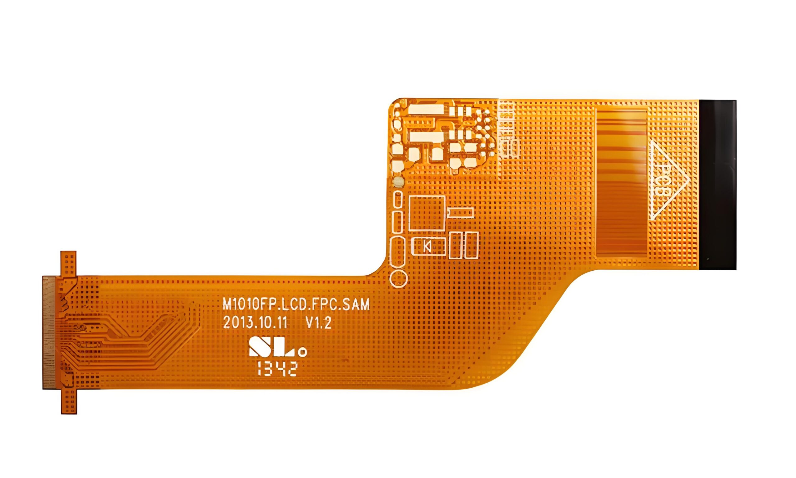
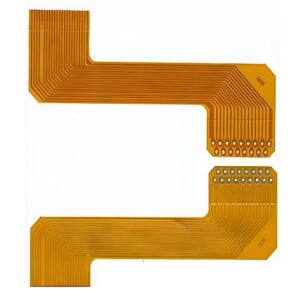
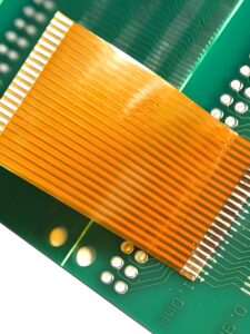
In the overall PCB design of mobile phones, the flexible printed circuit (FPC) used in foldable areas requires excellent flexibility. The Ministry of Information Industry mandates that foldable phones must withstand at least 50,000 folding cycles while leading global smartphone manufacturers require 80,000 to 100,000 cycles. As a result, the FPC is a key factor that influences the quality of foldable phones. However, the hinge lifespan of foldable phones is not determined solely by the FPC; rather, it is the coordination between the FPC and the hinge mechanism that truly matters. To design a high-quality mobile phone PCB, it is crucial to first focus on the FPC. Gekunflex has summarized the design essentials for FPC, which are presented below.
1) Material Selection:
To ensure bending performance, it is recommended to use a 0.5mil/0.5oz single-sided base material with rolled annealed (RA) copper. The cover layer should be 0.5mil thick.
2) Layer Selection:
Currently, color-screen phones generally use a 40-pin connector, with actual wiring ranging from 34 to 40 traces. The width of the FPC typically ranges between 3.2mm and 4mm. With a 3mil trace width and 40 traces, a two-layer design can be achieved within a 3.6mm width. A 0.5oz copper layer with 3mil traces can withstand a current of 70µA.
3) Trace Design for the Bending Area:
- a) No vias should be present in the bending area.
- b) Add protective copper traces on both outer sides of the circuit. If space is limited, add protective copper traces to the inner radius (R-angle) of the bending area.
- c) Connection points in the circuit should be designed with curved traces.
4) Bending Area Design (Air Gap):
A layered design should be used in the bending area, removing the adhesive to help distribute stress. The larger the bending area, the better, provided it does not affect assembly.
5) Shielding Layer Design:
Currently, mobile phone shielding layers typically use silver paste or copper foil, and some Japanese phones use silver foil.
- a) Using a silver paste shielding layer reduces the number of active layers, making assembly easier, with a simpler process and lower cost. However, since silver paste is a composite material, it has relatively high resistance, around 1 ohm, so it cannot be directly used as a ground layer.
- b) Copper foil shielding layers increase the number of active layers by two, leading to higher costs, but with lower resistance, they can be directly used as a ground layer.
- c) Silver foil shielding layers are too expensive to be practical.
6) Plating Selection:
To ensure bending performance, partial copper plating must be used. Full copper plating should be avoided.
Gekunflex has over 10 years of experience in PCB layout design, backed by a strong R&D engineering team. They assist customers and layout engineers in schematic analysis and PCB design, eliminating electrical design errors while ensuring design quality and reliability. Visit the Gekunflex website for more information.


Leave A Comment