Flexible PCB Assembly and Soldering Process for PCBA
introduction
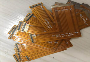
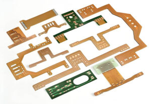
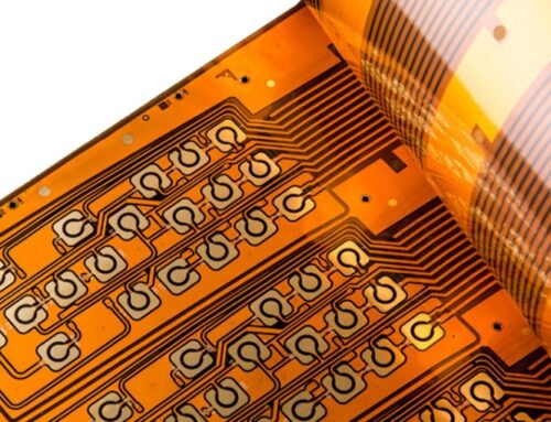
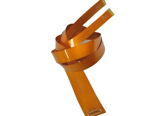
Flexible Printed Circuit (FPC), also known as flexible circuit boards, differs significantly from rigid circuit boards in terms of PCBA (Printed Circuit Board Assembly) assembly and soldering processes. Due to the flexibility and lack of rigidity in FPCs, special carrier boards must be used to ensure the FPC is securely fixed and transported through basic SMT (Surface Mount Technology) processes like printing, component placement, and reflow soldering.
Preprocessing of FPC
FPCs are typically soft and not vacuum-packed when leaving the factory. They can easily absorb moisture from the air during transportation and storage, which necessitates pre-baking before SMT processing to slowly and forcibly remove the absorbed moisture. Failure to do so can lead to delamination or blistering of the FPC due to the rapid vaporization of moisture under the high temperatures of reflow soldering.
The general baking conditions are 80-100°C for 4-8 hours. In special cases, the temperature can be increased to above 125°C, but the baking time should be correspondingly shortened. Before baking, it’s essential to conduct a small sample test to determine if the FPC can withstand the set baking temperature, or consult the FPC manufacturer for appropriate baking conditions. During baking, the FPCs should not be stacked too densely—10-20 panels per batch are suitable. If there is an isolation paper between the FPC panels provided by the manufacturer, confirm that this paper can withstand the baking temperature; if not, it should be removed before baking. After baking, the FPC should show no significant discoloration, deformation, or warping, and must pass IPQC (In-Process Quality Control) inspection before proceeding.
Manufacturing the Special Carrier Board
Using the circuit board’s CAD files, the positioning data of the FPC’s holes is read to manufacture a high-precision FPC positioning template and a special carrier board. The diameter of the positioning pins on the template must match the positioning holes on the carrier board and the FPC. Since some FPCs vary in thickness due to protective layers or design considerations, with some areas thicker or thinner than others, the connection between the carrier board and the FPC must be processed accordingly, such as grinding or slotting, to ensure the FPC remains flat during printing and placement. The carrier board material should be lightweight, strong, heat-resistant, and able to dissipate heat quickly, with minimal warping after multiple thermal shocks. Common materials include synthetic stone, aluminum, silicone boards, and special high-temperature-resistant magnetized steel plates.
Production Process
This section details the SMT points for FPC using a regular carrier board. When using silicone boards or magnetic fixtures, FPC fixation becomes much easier, as tape is not required, but the key points of printing, placement, and soldering processes remain the same.
Fixing the FPC
Before SMT, the FPC must be precisely fixed to the carrier board. It is crucial to minimize the time between fixing the FPC to the carrier board and proceeding with printing, placement, and soldering. There are carrier boards with and without positioning pins. For boards without positioning pins, a positioning template with pins must be used. The carrier board is first placed on the template’s pins, so the pins protrude through the holes in the carrier board. Then, the FPC is placed on the exposed pins, fixed with tape, and separated from the template for printing, placement, and soldering. Carrier boards with built-in spring-loaded pins about 1.5mm long allow for direct placement of the FPC onto the pins and fixing with tape. During printing, the spring-loaded pins are fully compressed by the stencil, ensuring no impact on the printing quality.
Method 1 (Single-sided tape fixation):
Use thin, high-temperature-resistant single-sided tape to fix the four sides of the FPC to the carrier board, preventing any shifting or warping. The tape should have moderate adhesive strength, be easy to peel off after reflow soldering and leave no residue on the FPC. An automatic tape dispenser can cut the tape to uniform lengths, improving efficiency, reducing costs, and minimizing waste.
Method 2 (Double-sided tape fixation):
First, apply high-temperature-resistant double-sided tape to the carrier board, then stick the FPC onto the tape. The tape’s adhesive strength should not be too high, as this can cause the FPC to tear when removed after reflow soldering. After multiple passes through the reflow oven, the adhesive strength of the double-sided tape will gradually decrease; it must be replaced when it can no longer reliably fix the FPC. This step is critical in preventing contamination of the FPC, and operators should wear finger cots during handling. The carrier board should be properly cleaned before reuse, using a non-woven cloth with a cleaning agent or an anti-static sticky roller to remove dust, solder balls, and other debris. Care should be taken when handling the FPC, as it is fragile and prone to creasing or breaking.
FPC Solder Paste Printing
FPCs do not have special requirements for the composition of solder paste; the size of solder balls and metal content depend on whether there are fine-pitch ICs on the FPC. However, FPCs have higher requirements for the printing performance of solder paste. The solder paste should have excellent thixotropy, easily release from the stencil, adhere firmly to the FPC surface, and not exhibit defects such as stencil clogging or post-printing collapse.
Since the carrier board holds the FPC, and the FPC has high-temperature-resistant tape for positioning, the FPC’s printing surface is not as flat as a PCB, and the thickness and hardness are inconsistent. Therefore, a polyurethane squeegee with a hardness of 80-90 degrees should be used instead of a metal squeegee. A solder paste printer with an optical positioning system is recommended; otherwise, print quality could be compromised. Although the FPC is fixed to the carrier board, there will always be small gaps between the FPC and the carrier board, making equipment parameter settings critical for good print quality.
The printing station is also a key point for preventing FPC contamination. Operators should wear finger cots, maintain cleanliness, and frequently clean the stencil to prevent solder paste from contaminating the FPC’s gold fingers and plated contacts.
FPC Component Placement
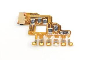
Depending on the product characteristics, component quantity, and placement efficiency, both medium and high-speed placement machines can be used. Since each FPC has optical MARK points for alignment, the SMD placement process on an FPC is similar to that on a PCB. However, despite being fixed on the carrier board, the FPC surface is not as flat as a PCB, and there will be local gaps between the FPC and the carrier board. Therefore, the placement machine’s nozzle descent height, blowing pressure, and movement speed must be precisely set. Additionally, FPCs are often panelized, and their yield rate is relatively low, so it is common to have defective pieces within a panel. This necessitates the placement machine’s BAD MARK recognition function to maintain production efficiency when not all boards in a panel are good.
FPC Reflow Soldering
A forced hot air convection infrared reflow oven should be used to ensure uniform temperature changes across the FPC, reducing the likelihood of soldering defects. If single-sided tape is used, only the four edges of the FPC are fixed, and the middle part may deform under the hot air, leading to tilted pads. This can cause molten solder to flow, resulting in cold solder joints, bridging, or solder balls, increasing the defect rate.
Temperature Curve Testing Method
Due to the carrier board’s heat absorption properties and the different types of components on the FPC, the temperature rise rate and heat absorption during reflow soldering vary. Carefully setting the reflow oven’s temperature profile is crucial for soldering quality. A reliable method is to place two loaded carrier boards before and after the test board during actual production, with the FPC on the test board populated with components. High-temperature solder wire is used to attach the temperature probe to the test points, and the probe wires are secured with high-temperature tape on the carrier board. Ensure the high-temperature tape does not cover the test points. Test points should be selected near the edges of the carrier board and on QFP leads for more accurate results.
Temperature Curve Setting
During oven temperature debugging, due to the FPC’s uneven heat distribution, it is advisable to use a temperature profile with a preheat/soak/reflow curve, as this allows easier control of the parameters in each temperature zone. Additionally, this approach reduces the thermal shock to the FPC and components. Based on experience, it is better to set the oven temperature to the lower limit of the solder paste’s technical requirements. The reflow oven’s airspeed should generally be set to the lowest possible, and the stability of the reflow oven’s conveyor chain is critical, with no jitter allowed.
FPC Inspection, Testing, and Depaneling
Due to the carrier board’s heat absorption, especially aluminum carrier boards, the temperature is relatively high when exiting the oven. It is advisable to add a forced cooling fan at the oven exit to speed up cooling. Operators should wear heat-resistant gloves to avoid burns from the hot carrier board. When removing the soldered FPC from the carrier board, apply even force and avoid excessive force to prevent tearing or creasing the FPC.
Inspect the removed FPC under a magnification of at least 5x, focusing on issues such as residual adhesive, discoloration, solder on the gold fingers, solder balls, and solder joints on IC leads. Due to the FPC’s uneven surface, AOI (Automated Optical Inspection) is prone to high false detection
rates. It is recommended to use a comprehensive test method combining AOI with manual inspection to reduce false detection and missed detection rates. Finally, after removing the FPC from the carrier board, the FPC should be sent for ICT (In-Circuit Testing) and FCT (Functional Circuit Testing) testing.
Some FPCs are spliced into a panel, and to facilitate subsequent processes like assembly, the panels should be separated. Depaneling methods include laser cutting, punching, and milling cutters. Laser cutting has the highest precision, with minimal dust or burrs, but can be slow and expensive. Punching is fast, but the mold is prone to damage, with easy dust formation. Milling cutters are efficient, but the cutters wear out quickly and are costly to maintain.
Conclusion
The assembly and soldering process for FPC in PCBA presents unique challenges due to the flexible nature of the circuit board. By ensuring proper preprocessing, utilizing appropriate carrier boards, and adhering to meticulous production processes, manufacturers can achieve high-quality, reliable FPC assemblies.




Leave A Comment