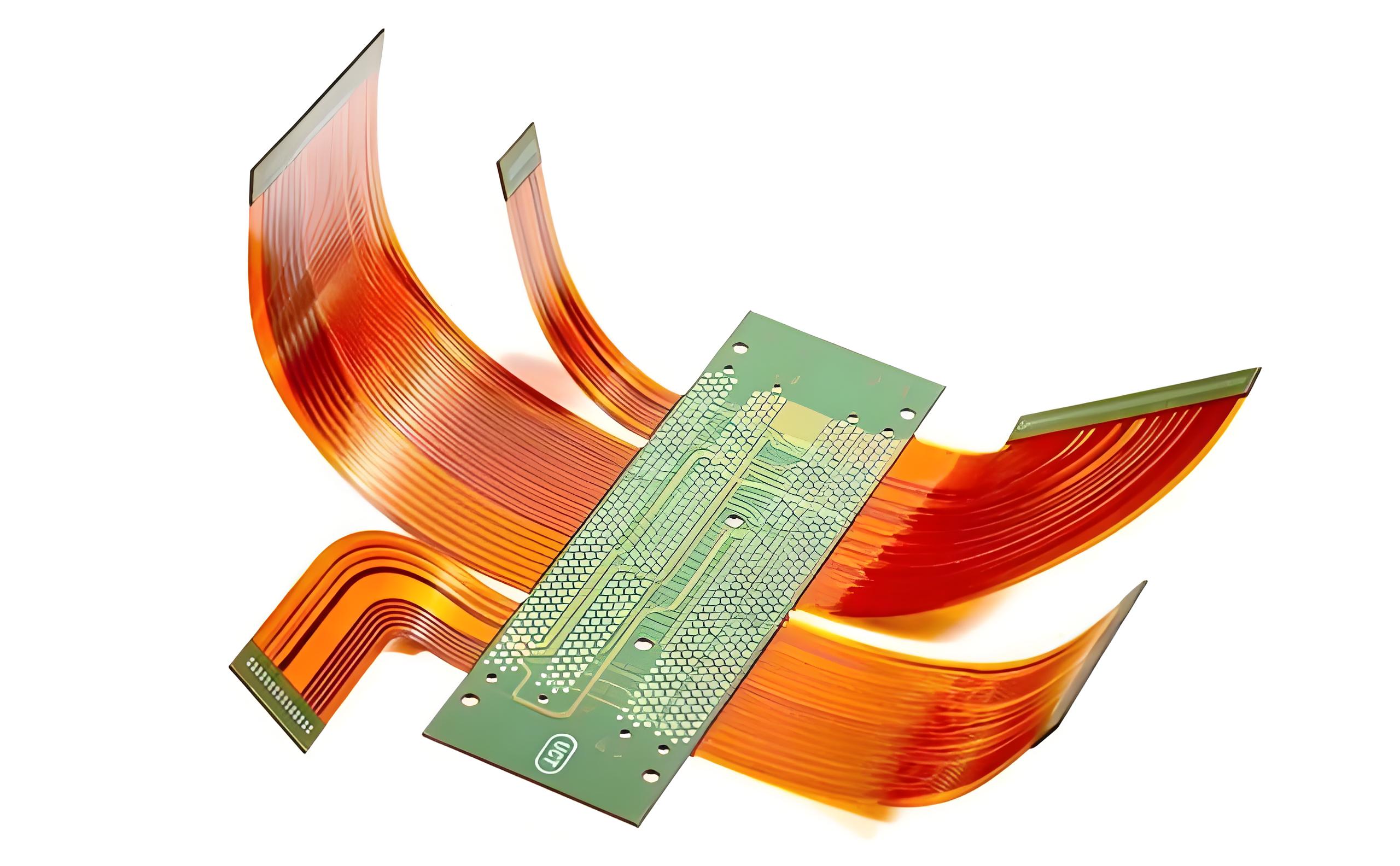
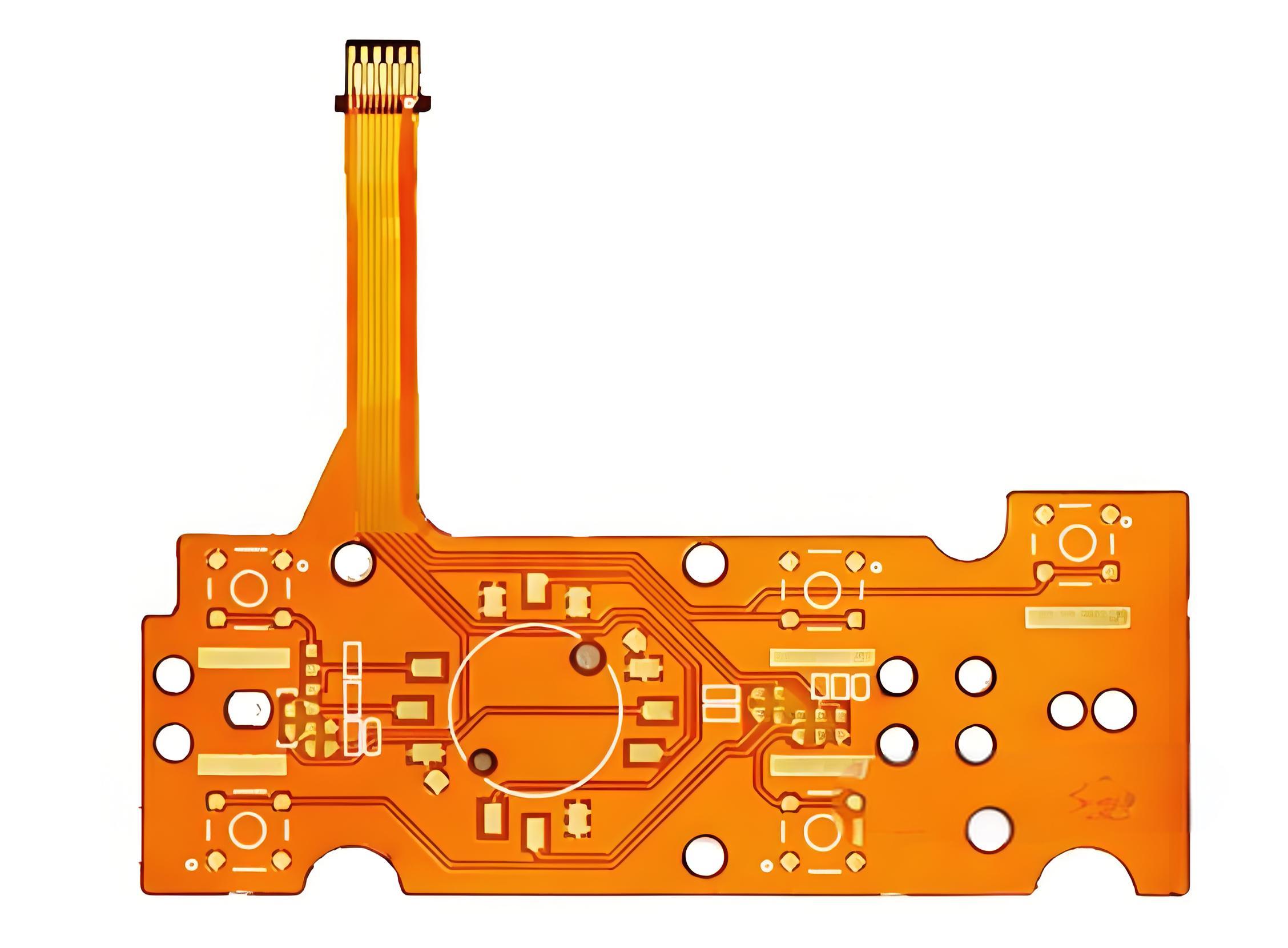
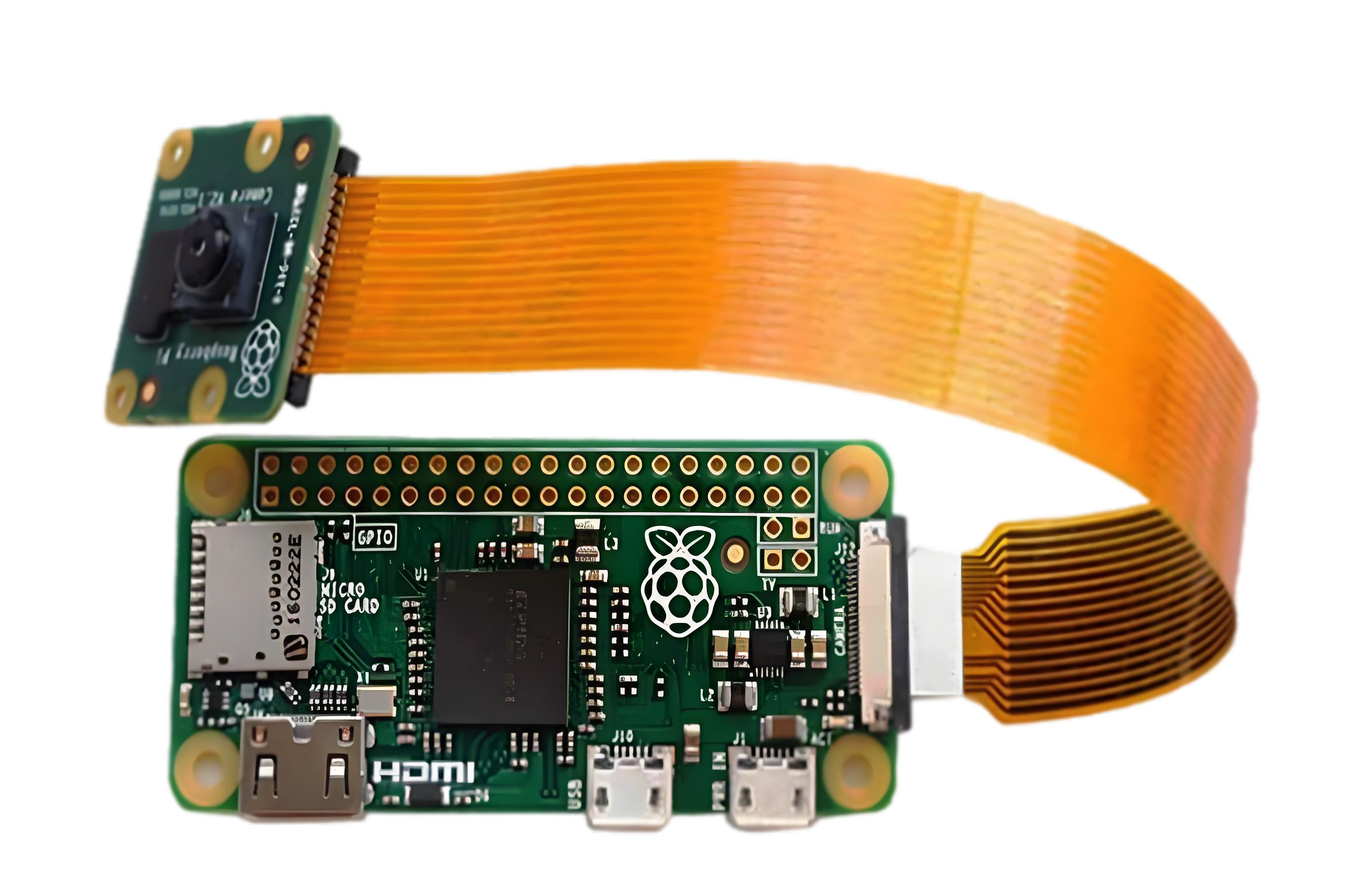
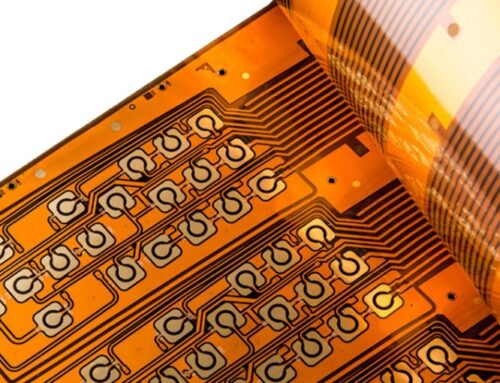
FPC, also known as Flexible Printed Circuit, Flex Circuit, or simply Flex Board, is made by etching copper foil on a substrate of polyester film or polyimide to form circuits. It is known for its high reliability and excellent flexibility.
Flexible circuit boards are small, lightweight, and highly flexible, allowing them to move and stretch freely in three-dimensional spaces. This integration of component assembly and wire connection meets the demand for PCB boards to become higher in density, smaller, lighter, and thinner.
Flexible circuit boards belong to a category of specialized materials, with certain technical thresholds operational difficulties, and higher costs. How are they produced? Let’s take a look at the production process of flexible circuit boards:
I. Single-Sided Board Production Process
Material Preparation → Drilling → Dry Film Application → Exposure → Developing → Etching → Film Removal → Lamination → Layer Pressing → Reinforcement → Curing → Surface Treatment → Silk Screen Printing → Punching → Final Inspection → Packaging → Shipment
II. Double-Sided Board Production Process
Material Preparation → Drilling → Copper Deposition → Copper Plating → Dry Film Application → Exposure → Developing → Etching → Film Removal → Lamination → Layer Pressing → Reinforcement → Curing → Surface Treatment → Silk Screen Printing → Punching → Final Inspection → Packaging → Shipment
Compared to single-sided boards, the double-sided board production process includes two additional steps: copper deposition and copper plating.
III. Process Explanation:
1. Material Preparation
FPC materials (substrates and cover films) are generally supplied in rolls, with a width of 250mm and a length of 100 meters. Since the length of the actual production boards is usually no more than 300mm, the materials need to be cut into smaller pieces, either manually or by machine, for production.
2. Drilling
Drill holes of specific sizes and quantities in the substrate, cover film, or reinforcement plate as required.
Note: Square or other irregular holes cannot be achieved by drilling and need to be punched with a steel mold or cut with a laser.
3. Copper Deposition
Form a thin layer of copper on the hole walls to provide an electrical path for subsequent copper plating. During copper deposition, Cu2+ ions are reduced to metallic copper and deposited on surfaces and hole walls. The copper thickness is about 0.5-2um.
4. Copper Plating
Since the copper thickness after deposition is only 0.5-2um, it needs to be thickened through copper plating to 12-30um.
5. Dry Film Application
Apply the dry film to the substrate with a certain pressure and temperature.
6. Exposure
Use light to transfer the circuit pattern from a photomask (film) to the dry film. The dry film exposed to light forms a protective layer, while the unexposed photoresist will be removed during development, revealing the copper to be etched.
7. Developing
Use a developer (sodium carbonate) to wash away the unexposed dry film, exposing the copper for etching or other processing.
8. Etching
Etch away the uncovered copper foil after developing it to form the desired circuit.
9. Film Removal
Remove the remaining dry film after etching, revealing the required circuit directly on the copper.
10. Reinforcement
To provide specific areas with increased thickness and rigidity for subsequent installation or assembly, attach a rigid reinforcement plate. The reinforcement plate can be stainless steel, aluminum, FR4, polyimide, polyester, etc.
11. Surface Treatment
Surface treatment prevents copper oxidation and provides a soldering or bonding layer. Common surface treatments include oxidation prevention (OSP), nickel-gold plating, immersion nickel-gold, tin plating, immersion tin, and immersion silver.
12. Final Inspection
Inspection methods include ① Visual inspection and ② Microscope inspection (at least 10x magnification). The main aspects checked are appearance, including scratches, dents, wrinkles, oxidation, bubbles, solder mask misalignment, drilling misalignment, circuit gaps, residual copper, foreign objects, etc.
13. Packaging
Packaging can be standard, anti-static, vacuum, or tray packaging.
This concludes Gekun’s overview of the FPC flexible circuit board production process. We hope it helps you. Gekun has a team of experienced PCB engineers who can provide high-quality FPC flexible circuit board prototyping services. We welcome customers to place orders and experience our service!




Leave A Comment