High-Density flex pcb board: Key Applications and Emerging Trends
Definition of High-Density FPC:
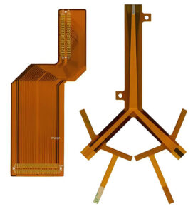
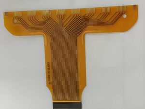
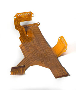
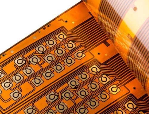
High-density flex pcb board is typically defined by the precision of fine lines and micro via processing capabilities. According to IPC standards, when the line spacing (pitch) is less than 150μm and the micro via diameter is smaller than 150μm, it qualifies as high-density FPC. Ultra-high-density FPC further reduces these dimensions. The applications of high-density FPCs can be categorized into several areas:
IC Substrates: Such as CSP and BGA
Information Products: Including hard disks and inkjet printers
Consumer Electronics: Such as cameras and mobile phones
Office Automation Products: Including fax machines
Medical Devices: Such as hearing aids and defibrillators
LCD Modules
In recent years, the demand for high-density FPCs has grown significantly compared to traditional FPCs. This article will provide an overview of some of the most in-demand high-density FPC applications.
Applications
TBGA (Tape Ball Grid Array)
The trend toward lightweight IC packaging has led many companies to design flexible circuits as IC substrates. Beyond high density, their superior thermal and electrical properties are key reasons for their use.
TBGA uses flexible circuits as IC carriers, providing fine lines and thin profiles. Currently, most TBGA applications use single-layer copper, with the use of double-layer metal gradually increasing. TBGA mass production sizes range from 11mm × 11mm to 42.5mm × 42.5mm, with pin counts from 100 to 768. The most common TBGA packages have 256 and 352 pins with a 35mm × 35mm size and are used in products such as microprocessors, chipsets, memory, DSP, ASICs, and PC network systems.
Chip Scale Package (CSP)
CSP, or Chip Scale Package, focuses on minimizing the size of the package relative to the chip. There are four main types: rigid substrates, lead frames, flexible substrates, and wafer-level packages. The flexible substrate, a high-density FPC, is used as the IC carrier. The key difference: TBGA’s fan-out method makes packages larger, while CSP’s fan-in keeps them within 1.2 times IC size. CSP ICs are used in flash memory, SLIM, ASICs, and DSPs, and are found in digital cameras, camcorders, mobile phones, and memory cards. The connection between the IC and the flexible carrier is typically achieved through wire bonding, though flip-chip methods are becoming more common. CSP package sizes range from 6mm × 6mm to 17mm × 17mm, with package spacing from 0.5mm to 1.0mm. Texas Instruments μStar BGA and Tessera’s μBGA are notable examples of flexible CSP packages.
LCD Driver IC Packaging
Traditionally, LCD driver ICs were packaged using high-density FPCs in a TAB (Tape Automatic Bonding) method. This involved using anisotropic conductive film (ACF) to connect the TAB external pins (bonded to the IC internally) to the LCD panel’s ITO electrodes, achieving a pitch as fine as 50μm. The TAB tape width commonly used is 48mm or 7mm, with typical I/O counts of 380, primarily used in mobile phones, camcorders, and laptops.
However, TAB-only LCD driver IC packaging limits the reduction in package size since passive components still require a separate PCB. The COF method mounts the driver IC and passive components on a flexible substrate, simplifying design and reducing size. COF has become a popular method for LCD packaging, with significant market potential, though challenges remain in achieving fine lines, thin profiles, and material adhesion.
Inkjet Printer Heads
The inkjet printer head drive circuits also use high-density flexible circuits, typically without adhesives. The common pitch resolution is around 150μm, with a trend toward even finer resolutions. Flexible circuits in this application commonly have a width of 24mm, and the market for these high-density FPCs is largely dominated by 3M.
Hard Disk Drive (HDD) Read/Write Heads
With the rapid development of data storage technologies driven by the growth of information, the internet, and digital imaging, the demand for increased storage capacity and access speed has grown significantly. HDDs for PCs, notebooks, automotive computers, GPS systems, digital cameras, and camcorders all require what is known as R/WFPC (read/write head FPC). The high-density design of these FPCs is critical, as they must operate in environments with temperatures up to 80°C and withstand high-speed dynamic vibrations without wire breakage, highlighting the stringent reliability requirements.
Development Trends and Technical Requirements
Fine Lines & Microvia
For applications like COF, the pitch will reduce to 25μm~50μm, challenging the substrate (copper adhesion, thickness), circuit processing (photolithography resolution, etching control, equipment transmission), and more. Microvia sizes will shrink to 50μm or smaller, and the demand for blind and buried vias will likely increase, driving the adoption of laser-based processes over traditional mechanical drilling.
Microvias
As via sizes decrease to 50μm, traditional mechanical drilling becomes inadequate, necessitating the use of laser drilling and direct etching of PI film. This method is commonly applied in IC substrates such as CSP and TAB.
Flying Leads
Some high-density FPCs with special structures allow for PI film to be etched away by dry or wet methods, leaving “flying leads” that can be directly bonded or soldered to rigid boards.
Small Coverlay Openings
As overlay opening resolution decreases to below 50μm, with an increasing number of openings, traditional punching methods become impractical. Thus, PIC (Photoimageable Coverlayer) technology has been developed to meet future demands.
Surface Finish
Lead-free processes such as chemical nickel-gold plating, electroplating, and pure tin, commonly used for rigid boards, are expected to become mainstream for flexible circuits as well.
Micropump Array
The reliability and density requirements of CSP, flip-chip, and similar technologies make micropump arrays a significant challenge in FPC manufacturing.
Dimensional Control
As miniaturization continues, precision must greatly improve. This will require careful consideration of material selection, layout design, equipment specifications, process control, and compensation design.
Inspection: AOI and Non-Contact Electrical Testing
Combining Automated Optical Inspection (AOI) with non-contact electrical testing is a potential solution for the inspection of high-density FPCs before shipment.
Conclusion
To maintain high growth rates and profitability, flexible circuits must evolve toward high-density applications. This evolution will require simultaneous advancements in materials, particularly the development of adhesive-less substrates and photo-imageable overlay films, which will play crucial roles in transitioning traditional flexible circuits to high-density FPCs.
China already has a strong foundation in IC and LCD packaging, with significant capabilities in FPC manufacturing. By leveraging its established IC and LCD panel manufacturing strengths, China has the opportunity to lead in the development of new packaging products and technologies. However, the development of new materials remains key to controlling costs and ensuring profitability. Coordinating upstream FPC material development with production processes will be essential to maintaining this competitive advantage.





Leave A Comment