PCB Assembly Services: Unveiling the Green Charm of PCBs
Understanding the Green in PCBs
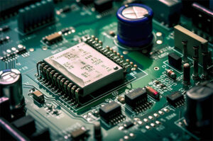
PCBs, typically green in color, serve as the rigid foundation onto which various electronic components are soldered during a process called “PCB Assembly” or PCBA. A PCB is composed of a substrate made from fiberglass, copper layers that form the traces, holes for components, and multiple layers, which can include both inner and outer layers.
The substrate and components are insulated with a solder mask and bonded together using epoxy resin. This solder mask can be green, blue, or red, commonly seen in PCB colors. The solder mask prevents components from shorting out with traces or other components.

Copper Traces and Their Role
Copper traces are used to transfer electronic signals from one point to another on the PCB. These signals can be high-speed digital or discrete analog signals. These traces can be made thick to provide power for powering components.
In most PCBs providing high voltage or current, there is a separate ground plane. Components on the top layer are connected to internal GND planes or internal signal layers through “vias.”
Assembling Components: The Core of PCB Functionality
Components are assembled on the PCB to enable it to function according to design. The functionality of the PCB is paramount. Even a tiny misplacement of an SMT resistor or a small cut in a trace can render the PCB non-functional. Therefore, assembling components correctly is crucial. A PCB with assembled components is known as a PCBA or an assembled PCB.
The complexity or simplicity of a PCB’s functionality depends on the specifications described by the customer or user. PCB sizes also vary according to requirements.
The PCB assembly services involves both automated and manual processes, which will be discussed in detail.
PCB Layers and Design
As mentioned earlier, there are multiple signal layers between the outer layers. Let’s discuss the types of outer layers and their functions.
1. Substrate: Made from FR-4 material, this rigid board is where components are “populated” or soldered. It provides rigidity to the PCB.
2. Copper Layer: Thin copper foil is applied to the top and bottom to create the top and bottom copper traces on the PCB.
3. Solder Mask: This is a layer applied to the top and bottom of the PCB. It is used to create non-conductive areas on the PCB, isolating copper traces from each other and protecting against short circuits. The solder mask also prevents unwanted parts from being soldered and ensures that solder flows into the area where soldering is intended, such as holes and pads. These holes connect THT components to the PCB, while PADs are used to secure SMT components.
4. Silkscreen: The white labels we see on PCBs, such as R1, C1, or some description on the PCB or company logo, are all made from the silkscreen layer. This silkscreen layer provides important information about the PCB.

Types of Assembly Techniques
SMT (Surface Mount Technology):
SMT component assembly is difficult for human hands and can be time-consuming, so automated pick-and-place robots mainly do it.
THT (Through-Hole Technology):
Components with leads and wires include resistors, capacitors, inductors, PDIP ICs, transformers, transistors, IGBTs, and MOSFETs.Components must be inserted on one side of the PCB, with the legs pulled on the other side, cut, and soldered. THT component assembly is usually done by hand soldering and is relatively easy.
Assembly Process Prerequisites
Before the actual PCB manufacturing and assembly process begins, manufacturers check the PCB for any defects or errors that may lead to failure. This process is called Design for Manufacturing (DFM). Manufacturers must follow these basic DFM steps to ensure a flawless PCB.
Component Layout Considerations:
Through-holes must be checked for polarized components. The polarity of components like electrolytic capacitors, diode anode and cathode, and SMT tantalum capacitors must be checked. The IC notch/head direction must be checked. Components requiring heatsinks should have enough space to accommodate other components so that the heatsink doesn’t touch them.
Hole and Via Spacing:
The spacing between holes and between holes and traces should be checked. Pads and vias should not overlap.
Copper Pads, Thickness, and Trace Widths should be considered:
After performing the DFM check, manufacturers can easily reduce manufacturing costs by minimizing the number of scrap boards. This helps quickly move through the process by avoiding failures at the DFM level.
Step-by-Step PCB Assembly Services:
Apply Solder Paste Using a Stencil
First, solder paste is applied to the areas on the PCB that are appropriate for the components. This is done by applying solder paste onto a stainless steel stencil. The stencil and PCB are fixed together using mechanical clamps, and then the paste is uniformly applied to all the openings on the board using an applicator. The paste is evenly spread by the applicator. Thus, the correct amount of paste must be used in the applicator. When the applicator is removed, the paste will remain in the desired areas of the PCB. The gray solder paste is 96.5% tin, containing 3% silver and 0.5% copper, which is lead-free. This solder paste will melt during the heating process in Step 3, creating a strong joint.
Automatic Placement of Components
The second step in PCBA is the automatic placement of SMT components on the PCB. This is done using pick-and-place robots. At the design level, designers create a file provided to the automation robots. This file has pre-programmed X, and Y coordinates of each component used in the PCB and identifies the location of all components. Using this information, the robot simply places the SMD devices accurately on the board. The pick-and-place robot picks up the components from its vacuum grippers and places them accurately on the solder paste.
As the technology matured, the automated robots for pick-and-place components relieved the technicians of their workload, enabling fast and accurate component placement. These robots can work around the clock without fatigue.
Reflow Soldering
After placing the components and applying solder paste, the third step is reflow soldering. Reflow soldering involves placing the PCB with the components on a conveyor belt. The conveyor belt then moves the PCB and components into a large oven that generates a temperature of 250°C. This temperature is sufficient to melt the solder. The molten solder will then fix the components onto the PCB and form joints. After being subjected to high temperatures, the PCB is moved into coolers. These coolers cure the solder joints in a controlled manner. This establishes a permanent connection between the SMT components and the PCB. In the case of double-sided PCBs, the side with fewer or smaller components will first be placed on the conveyor. After the reflow soldering process for the first side, the PCB is reversed, and the process is repeated.

Inspection of Soldered Components
The fourth step is inspecting the PCB to verify proper soldering, component placement, and quality control. In SMT assembly, three main types of inspections are conducted: manual inspection, Automatic Optical Inspection (AOI), and X-ray Inspection.
Manual Inspection:
Manual inspection is done for small batches where components and boards can be examined using magnifying glasses to spot errors.
Automatic Optical Inspection (AOI):
In large-scale production, AOI is performed after reflow soldering. AOI machines are faster and more efficient at spotting errors in components. These AOI machines contain several cameras that can view the PCB from multiple angles. The images from different angles are then combined to detect soldering defects, incorrect component placements, or missing components.
X-ray Inspection:
For large-scale production of multilayer PCBs, X-ray inspection is the preferred method. In a multilayer PCB, solder joints may be covered under components or other layers. X-ray inspection can spot hidden joints and defects that would otherwise go unnoticed.
Insertion of Through-Hole Components (THT)
After soldering all SMT components, the fifth step in PCB assembly is inserting Through-Hole Components (THT). The first step is inserting THT components, which include resistors, capacitors, and other components with leads, into the through holes on the PCB. After inserting, the PCB is flipped upside down so that the leads come out on the bottom side. These components are then soldered onto the PCB by applying molten solder to the PCB. This is done in two ways: using a wave soldering technique or manually by soldering iron.
Testing
After the PCB is fully assembled, the final step is testing it to verify its functionality. Testing is done through “In-Circuit Testing” (ICT) or by running functional tests.
In-Circuit Testing (ICT):
In ICT, the board is placed on a bed of pins, where each pin is programmed to check the functionality of the IC, such as measuring voltage and checking all connections. This ensures the circuit functions as intended. The board can be tested individually for its functionality and performance if it passes this test.
Functional Testing:
Functional testing is done when the PCB assembly is finished, and the assembled PCB is powered on for the first time. After powering on, inputs are given, and the circuit is monitored to see if it provides the desired output.

Conclusion
The PCB Assembly Services is an intricate and precise procedure involving multiple stages, from solder paste application to final testing. Each step is crucial in ensuring the functionality and reliability of the final PCB. With advancements in technology, the assembly process has become more automated, reducing the likelihood of errors and increasing efficiency. Whether it’s a simple single-layer PCB or a complex multilayer board, the principles of PCB Assembly Services remain consistent, focusing on precision, quality, and functionality.


Leave A Comment