PCB Board Assembly Jobs: From Design to Final Testing
Unveiling the Birth of a PCB: From Inspiration to Reality
Ignition of Creativity and Circuit Diagram Drafting
In the world of electronic engineering, the creation of every PCB begins with a designer’s spark of inspiration. Designers use their expertise to translate abstract electronic concepts into precise circuit diagrams. These blueprints form the foundation of PCB assembly, guiding the layout and connections of electronic components. Professional design software plays a critical role in this process, offering advanced features such as auto-routing and signal integrity analysis, which significantly improve the accuracy and efficiency of the design.
Prototype Development: The Transition from Blueprint to Physical Reality
Once the design phase is complete, the next step is prototype development, which transforms two-dimensional circuit diagrams into three-dimensional physical PCBs. Prototyping is crucial for verifying the feasibility of the design, allowing engineers to test and fine-tune the design before actual assembly. This phase presents challenges, as engineers must address issues such as signal interference, component compatibility, and thermal management. However, overcoming these challenges fosters creativity and innovation in PCB assembly technology.
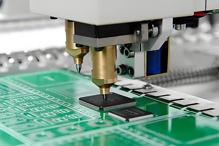
PCB Assembly: The Fusion of Precision and Craftsmanship
In the design and assembly of PCB boards, selecting components is crucial as it directly impacts the circuit board’s performance, reliability, and cost. Key factors to consider include:
Pads, vias, mounting holes, traces, connectors, fills, and electrical boundaries: These fundamental parts form the base structure of the PCB, with their selection and layout affecting both electrical performance and mechanical strength.
Component Layout: Follow the principle of “place large components first, then smaller ones; place complex components before simpler ones.” Prioritize critical circuit units and core components. The layout should refer to the schematic diagram and arrange major components according to the board’s main signal flow direction. Additionally, component arrangement should facilitate debugging and maintenance, avoiding situations where larger ones obscure small components, and ensuring sufficient space around components that require debugging.
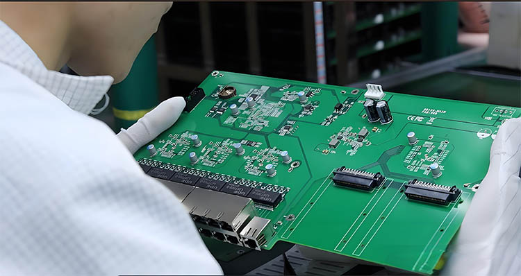
Quality Inspection: The Perfect Guardian of PCB Assembly
Testing Process: Layered Safeguards to Ensure Quality
In PCB board assembly jobs, quality inspection is essential to ensuring every circuit board is flawless. The process begins with a meticulous preliminary inspection, where engineers examine each solder joint and component for precision. This is followed by functional testing, where the circuit board is tested under various simulated conditions to verify stable operation according to design specifications. Electrical tests, such as continuity testing and insulation resistance testing, reveal potential issues and detect minor defects that might affect performance. Quality inspection is a critical factor in enhancing product reliability and customer satisfaction.
Problem Solving: Sparks of Wisdom and Continuous Improvement
Engineers often face challenges during quality inspection, such as soldering defects, component failures, or design oversights. To address these issues, they use advanced diagnostic tools like X-ray inspection and thermal imaging technology to quickly locate and resolve problems. These tools help detect defects not visible to the naked eye and improve problem-solving efficiency. A culture of continuous improvement is vital, motivating teams to learn and innovate to enhance inspection accuracy and overall product quality.
Quality Inspection Methods for PCBA Circuit Boards After Soldering
Visual Inspection:
This basic method focuses on the appearance of the circuit board, checking solder quality, component installation, and potential damage. Inspections are typically done with the naked eye or under a microscope. Standards require no obvious burns, normal solder shapes, and no cold solder joints, open joints, or missed soldering. Components should be properly aligned, not tilted or displaced, and all soldering points, wires, and connectors should have no exposed copper. Components should be securely soldered with no damage due to excessive heating.
Electrical Testing:
Electrical performance testing involves measuring voltage, current, and impedance at various points on the circuit board to ensure proper functioning. Electrical parameters must fall within specified ranges according to design requirements. Test fixtures and interfaces are used to perform electrical tests, ensuring all connectors and solder joints are correctly connected.
The Future of PCBs: Innovation and Sustainability
Several trends are shaping the future of the PCB industry:
Technological Advancements: HDI PCBs and FCBs are making circuit boards smaller and more complex, while trends like 5G integration demand more robust, specialized PCBs. Balancing size constraints with growing performance requirements remains a challenge.
Manufacturing Progress:
Technologies such as SMT, 3D printing, and AI-based inspection systems promise to enhance automation, reduce costs, improve sustainability, and strengthen quality control.
The future of PCBs will likely involve a convergence of these trends, leading to exciting advancements in PCB technology in the coming years.
Conclusion
PCB Assembly is a display of technical skill and an unwavering pursuit of detail and quality. Behind every successful circuit board lies the dedication and expertise of engineers. With ongoing technological advancements, PCB assembly processes will become even more refined, promising an exciting future for the electronic world.


Leave A Comment