PCB Printed Circuit Board Assembly: the art and science
introduction
PCB printed circuit board assembly transforms abstract design concepts into tangible electronic products, serving as the cornerstone of electronic innovation. In the rapidly changing wave of technology, PCB assembly technology is not only a showcase of precision engineering but also a perfect fusion of technology and art. From design sketches to the birth of finished products, every step reflects the engineers’ relentless pursuit of craftsmanship.
In the world of PCBs, details are crucial. Designers cleverly arrange electronic components within confined spaces to maximize circuit performance. The use of automation technology during the manufacturing process ensures precise placement of components and flawless soldering. Stringent quality testing guarantees the reliability and durability of every PCB.
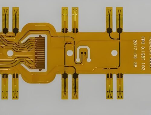
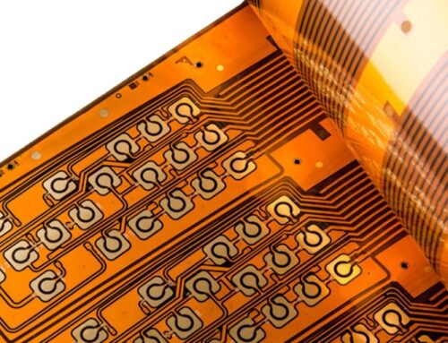
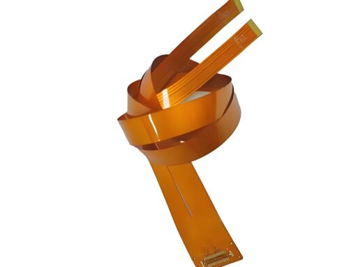
Continuous technological advancements drive innovation in PCB assembly technology. The application of emerging technologies like 3D printing and flexible circuit boards brings endless possibilities to PCB assembly, hinting at the future development direction of electronic devices. This article delves into the intricate craftsmanship of PCB printed circuit board assembly, revealing how it merges innovative thinking with cutting-edge technology to create remarkable electronic products.
Exploring PCB Printed Circuit Board Assembly: A Milestone in Electronic Innovation
In the wondrous world of modern electronic technology, PCB printed circuit board assembly plays an indispensable role. As the backbone of electronic components, the history of PCB development encapsulates the evolution of electronic devices. From the early days of single-layer boards to today’s widely used multilayer, flexible, and rigid-flex boards, the evolution of PCB technology continually pushes the limits of electronic device performance and size.
The Revolution of PCB in History
Looking back, the birth of PCB printed circuit board assembly technology can be traced back to the 1930s. At that time, engineers focused on the complexity of connecting electronic device components and began exploring a new method of printing electronic pathways onto insulating boards. This not only greatly simplified the assembly process of electronic devices but also significantly enhanced their reliability and durability.
As time progressed, PCB technology underwent a series of revolutionary changes. Innovations from single-layer boards to double-layer and multilayer boards, along with breakthroughs in flexible and rigid-flex boards, brought transformative changes to the design and production of electronic devices. These innovations made electronic devices thinner and more powerful, while also realizing the miniaturization and integration of electronic equipment.
PCB Technology: The Harmony of Precision and Creativity
As engineers engage in the process of PCB printed circuit board assembly, they act like artists, precisely designing circuit diagrams and carefully selecting materials and manufacturing processes to ensure the circuit’s excellent performance and reliability. With continuous technological advancements, automated and intelligent assembly technologies are continually enhancing production efficiency and assembly quality.
PCB Assembly: The Driving Force of Innovation
PCB printed circuit board assembly not only represents the forefront of electronic manufacturing but also serves as the core force driving the development of electronic technology. Every technological innovation brings new possibilities to the electronic world, making our devices smarter and our lives more convenient.
The Art of Design: The Subtlety of PCB Layout
In the grand blueprint of PCB printed circuit board assembly, the design phase is undoubtedly a crucial part. Designers are tasked with transforming abstract circuit diagrams into concrete and practical PCB layouts. They must find the perfect balance between circuit performance, cost, reliability, and future maintainability.
An excellent PCB design balances aesthetics with practicality. Designers, like artists on a canvas, carefully arrange electronic components in limited spaces to ensure efficient and stable signal transmission. This not only requires designers to have a deep knowledge of electronic engineering but also demands innovative thinking and meticulous attention to detail.
The Science of Manufacturing: The Precise Craftsmanship of PCB Assembly
In the intricate world of PCB printed circuit board assembly, the manufacturing process is a perfect exhibition of science and technology. Every step, from etching the circuit board to drilling holes and precisely placing components, demands high levels of precision and control. This process affects not only the physical form of the PCB but also directly impacts the performance and reliability of electronic products.
The application of modern automation equipment and intelligent systems has brought revolutionary changes to PCB printed circuit board assembly. Automated production lines can accurately control the etching process, ensuring the clarity and consistency of circuit patterns. Drilling machines can precisely drill the necessary holes in the circuit board, laying a solid foundation for subsequent component installation.
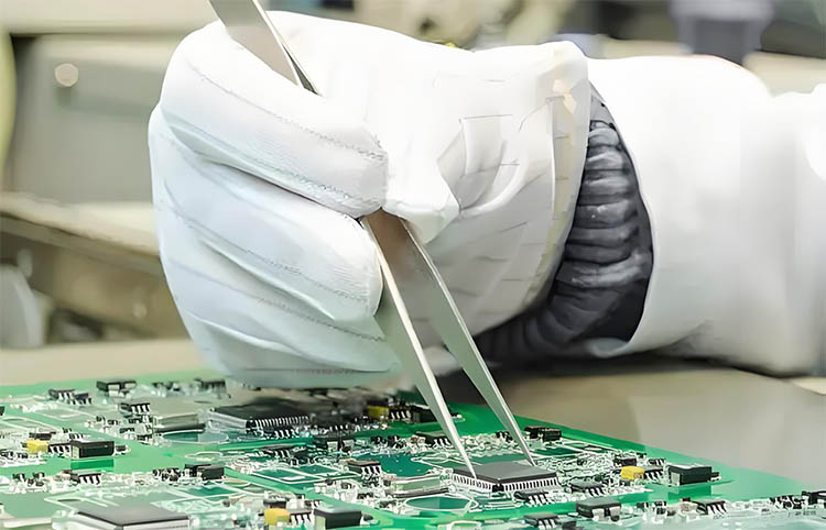
The placement stage further tests the precision of technology. High-speed placement machines can accurately position tiny electronic components at an astonishing speed. This level of precision is achieved through advanced visual recognition technology and precise mechanical control.
Quality Assurance: Testing and Verification in PCB Assembly
In the journey of PCB printed circuit board assembly, after the precision manufacturing process concludes, we arrive at the crucial phase of quality assurance—testing and verification. This series of rigorous inspection steps is a necessary trial that every PCB must undergo before moving from the production line to electronic devices.
Functional testing
First, functional testing is fundamental. It ensures that each electronic component operates as expected, with no short circuits or open circuits. Next, performance testing further verifies the electrical characteristics of the PCB in real-world applications, including signal integrity and circuit stability. These tests are vital for assessing whether the PCB meets design specifications.
Environmental adaptability testing
Environmental adaptability testing simulates various environmental conditions the PCB may encounter, from temperature variations to humidity impacts, and even vibrations and shocks. Through these tests, we can ensure that the PCB maintains its performance under various conditions, thereby guaranteeing the reliability of the final product.
Throughout the testing process, automated testing equipment plays a significant role. It not only enhances testing efficiency but also ensures the consistency and accuracy of the results. The quality control team supervises the entire testing process, ensuring that every PCB meets the highest quality standards.
Only when the PCB has passed all these tests can it be deemed a qualified product and subsequently used in the assembly of final electronic devices? This not only ensures the quality of PCB printed circuit board assembly but also represents a commitment to consumer safety and satisfaction. Through these meticulous tests and verifications, we ensure that every aspect of electronic products meets the highest standards.
Trends in the PCB Industry
Upgrading Downstream Demand Increases PCB Process Complexity
With the rapid expansion and ongoing upgrades of downstream application markets, PCBs are developing towards miniaturization, lightweight, multifunctionality, and high-speed/high-frequency characteristics. In the consumer electronics sector, devices like smartphones and tablets continue to evolve towards smaller sizes and diverse functionalities, requiring more components and ongoing size reduction on PCBs. In the computer and server sector, the further evolution of the 5G-A era and the rise of artificial intelligence technology have significantly enhanced communication frequencies and data transmission speeds, shifting the demand for PCBs towards high-speed and high-frequency specifications. Currently, servers/storage require six to sixteen-layer boards and packaging substrates, with high-end server motherboards exceeding sixteen layers and backplanes exceeding twenty layers. As server demand continues to rise, the technical level of PCBs must also evolve.
AI Trends Drive Server PCB Volume and Price Increases
Since 2023, several major events and breakthroughs have occurred in the field of artificial intelligence, highlighted by the release of cutting-edge large language models such as OpenAI’s GPT-4, showcasing exceptional capabilities in natural language processing and creative content generation. Google and OpenAI released Gemini 1.5 and Sora, surpassing expectations and highlighting increased competition in AI development. In the competitive AI landscape, high-speed communication thrives, making the PCB industry crucial as a supporting hardware field. Looking forward, as server platforms are updated and AI applications gradually materialize, the server sector will continue to proliferate, driving increases in PCB layer counts, materials, and process optimizations, achieving simultaneous volume and price increases. The increase in server information transmission rates necessitates the use of higher-layer boards and lower-loss materials; manufacturers need to increase layers to enhance resistance and achieve high-speed information transmission between chips, making higher-layer boards and lower-loss materials the primary growth market.
Conclusion
PCB printed circuit board assembly is the core of electronic manufacturing, covering design, precise manufacturing, and rigorous testing. Ongoing innovation in this field enhances electronic product performance and indicates vast potential for future technological breakthroughs. On the stage of the electronic industry, PCB assembly is undoubtedly a key force for progress.





Leave A Comment