Rigid-Flex PCBs Design: Strategies for Enhanced Performance and Reliability
Introduction
PCB design is trending towards lighter, thinner, and smaller formats. Besides high-density circuit board designs, the complex and vital field of three-dimensional interconnected assembly using rigid-flex PCBs is gaining prominence. These PCBs, combining flexible and rigid sections, are becoming indispensable in numerous applications. As a leading player in the PCB industry, Gekun provides comprehensive solutions that cater to the evolving demands of modern electronic designs.

What Are Rigid-Flex PCBs?
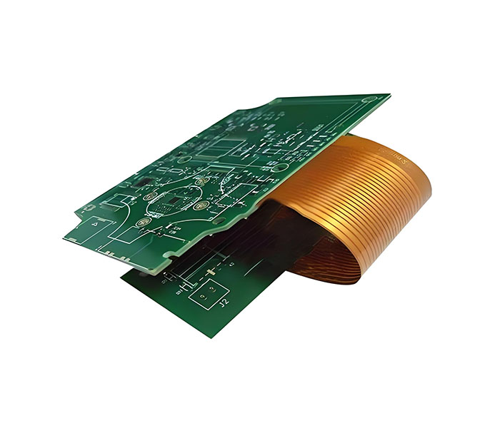
Rigid-flex PCBs integrate flexible circuit sections with traditional rigid circuit boards, forming a single unit that offers the benefits of both technologies. This combination results in a PCB that features both flexible and rigid areas, significantly saving internal space, reducing product volume, and enhancing performance. Such designs are particularly useful in products with specific spatial requirements.
Structure of Rigid-Flex PCBs
Rigid-flex PCBs consist of flexible substrates bonded with one or more rigid layers. The circuits on these layers are interconnected through metallization. Each rigid-flex PCB typically has multiple rigid sections and at least one flexible section. The design, which can involve more than one layer, allows for diverse applications and greater flexibility.
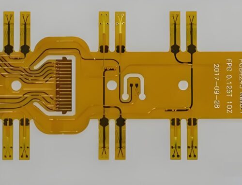
Manufacturing Process of Rigid-Flex PCBs
Creating rigid-flex PCBs requires both FPC and PCB manufacturing capabilities. The process begins with an electronics engineer designing the circuits and outlines. These designs are then processed by CAM engineers, followed by production on FPC and PCB lines. The flexible and rigid boards are seamlessly laminated together, resulting in the final rigid-flex PCB through a series of detailed steps.

Design Guidelines for Rigid-Flex PCBs
Designing rigid-flex PCBs is more complex than traditional PCBs and involves several critical considerations, especially in the transition zones and related routing and via placement.
Via Placement
Avoid using vias on the flexible sections during dynamic use, as bending can damage them. Vias should maintain a distance from the rigid-flex junctions, with a minimum of 50 mils for general applications and 70 mils for high-reliability scenarios. Most manufacturers won’t accept distances below 30 miles.
Pad and Via Design
Design pads and vias to maximize their size within electrical requirements. Transitions between pads and conductors should be smooth, avoiding sharp angles. Reinforce independent pads with pad fillets to enhance support. Ensuring larger solder mask reliefs and using teardrops on vias and pads can reduce the risk of damage.
Trace Design
In flexible sections, traces on different layers should not follow the same path to avoid mechanical stress during bending. Instead, stagger the traces. Round traces are preferred in flexible areas to reduce stress, contrasting with the typical rigid PCB design.
Copper Pour Design
To enhance flexibility, copper pours should use a mesh pattern, although solid copper may be needed for impedance control. Designers must balance electrical performance with mechanical flexibility based on specific requirements.
Drill to Copper Distance
A minimum distance of 10 mils should be maintained between drilled holes and copper. This distance ensures proper manufacturing and avoids issues, particularly in the rigid-flex junctions.
Rigid-Flex Transition Zone Design
The flexible section should ideally be in the middle of the layer stack and connected to the rigid sections, with vias considered buried vias. The design should ensure smooth transitions, perpendicular trace directions to the bending axis, and uniform trace distribution.
Bend Radius in Flex Zones
Rigid-flex PCBs should endure up to 100,000 flex cycles without failure. The bend radius design should consider the flexible section’s thickness and number of layers, following the formula R = W x T (where T is the total thickness, and W varies by layer count). Minimum bend radius standards should be 6 times the thickness for single-layer, 12 times for double-layer, and 24 times for multi-layer boards.

Conclusion
Designing rigid-flex PCBs requires meticulous attention to detail, particularly in flexible circuit design. Considerations include the base materials, adhesive layers, copper foils, cover layers, and reinforcement plates, each affecting performance parameters like peel strength and flexural endurance. Gekun delivers cutting-edge solutions that meet the stringent demands of modern electronics, ensuring optimal performance and reliability in every application.


Leave A Comment