What should be paid attention to in the process of rigid flex PCB design?
introduction
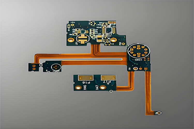
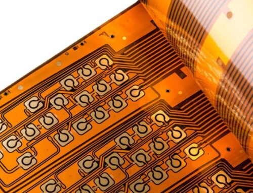
Traditional rigid flex PCB design consists of external rigid circuit board material layers and sandwich flexible board stack layers. PTH (Plated Through Hole) endpoints are used for inter-layer interconnections and connecting internal circuits to the external rigid areas. These rigid surfaces have only simple pads without conductor arrangements or other conductive areas, as their purpose is to protect all circuits from connections, short circuits, and damage caused during assembly.
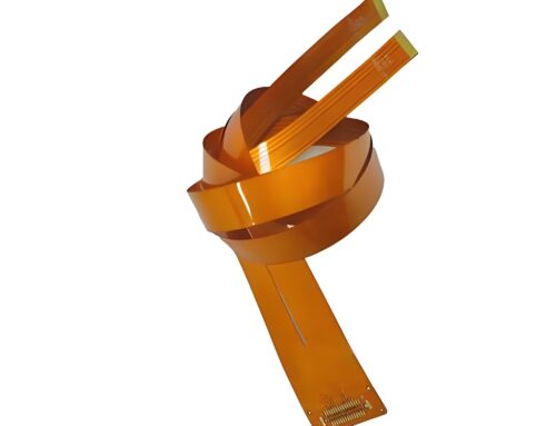
All connectors or hardware attachments occur in rigid areas, which also provide support for the circuits, strain relief, and component support. Interconnections between rigid areas rely on other flexible board layers, which are individually covered with protective films but generally do not fully connect with other flexible boards, allowing for better flexibility and reduced bending stress.
Rigid Flex PCB design Approach
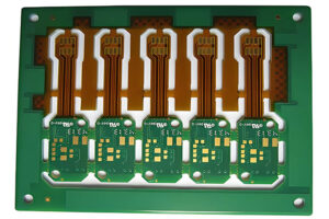
Rigid-flex PCBs are made in sheet form and only undergo cutting once both rigid and flexible areas are completed. Before this stage, the layered dielectric is assembled through processing, and the designer can ensure that all layers have equal support. For any flexible board process, a mechanical layout will be established to accurately construct all endpoints, reorganize the circuit list based on the types of circuits and graphic arrangements, determine the overall form of the flexible board, set design criteria, and routing while considering additional factors, including:
- Confirming the shape of the flexible and rigid boards.
- Special tool slots, windows, and bevels.
- Deciding on the flexible board areas: single-sided or double-sided, adhered or not.
- Material selection.
- Specifications.
The design of the mechanical structure layers adheres to wire bundle tolerance processing. The dimensions of the overall rigid board area can be handled according to the tolerance levels of NC (Numerical Control) machinery, while the flexible board layers between rigid areas require local tolerance handling. The layout of flexible boards between rigid areas should provide expansion compensation, but care must be taken to note that multiple flexible board layers may interfere with each other during assembly.
Design Process and Considerations
Use appropriate lengths of flexible board between rigid areas to achieve similar stress reduction without increasing manufacturing complexity. Single-sided adhered flexible layers are softer than double-sided ones but may increase manufacturing costs. They are commonly used designs in stacked structures but are recommended only as a reference for suppliers. Suppliers tend to provide competitive stacking techniques, but understanding the future practical limitations of the stacking design may also influence their judgments.
The flexible board pads shouldn’t be exposed after lamination; the rigid-flex PCB requires a PTH process, and exposed pads may complicate the manufacturing process, especially if surface solder coating is required. As the final process for rigid-flex PCBs requires cutting, complex circuits and excessive exposed areas can easily be damaged. Solder surfaces may crack under lamination temperatures, potentially rendering solder pads unsolderable, hence solder should be applied after lamination. If exposed pads are sealed within the sheet structure during plasma, electroless plating, immersion plating, and reflow soldering, they will be better protected as long as they only appear after the initial cutting.
Importance of Accurate Alignment and Inter-layer Registration
For multilayer products, especially high-value rigid-flex PCBs, ensuring precise alignment and registration between layers is critical. In such high-value products, material costs are not the primary consideration, and excessive circuit protection can lead to increased distances between contacts, which may not be economically viable.
Application of Post-Etching-Stamping Technology
To achieve precise inter-layer registration, the use of post-etching-stamping technology is recommended. This method accurately controls etching and protective film tool holes by setting multiple optical targets in each layer. During the processing, especially in stacking, post-etching, cutting, and other steps, variations in size may affect overall quality; thus, using smaller pieces can reduce this impact.
Stability and Tolerance Handling of Rigid Areas
The stability of rigid areas is vital for the overall structural integrity. By surrounding rigid areas with tool pins, the stability of copper panels can be enhanced. Additionally, handling group tolerances separately for rigid areas can improve yield rates and distribute the costs of extra tool pins or lamination fixtures.
Thickness Uniformity and Challenges in PTH Processing
Maintaining uniform thickness in rigid areas during the manufacturing of rigid-flex PCBs is necessary. Areas of differing thickness cannot undergo the PTH process simultaneously, potentially increasing costs. If interconnecting flexible boards to rigid areas is not necessary, using rigid film instead can help maintain thickness uniformity. Furthermore, PTH points should be at least 0.125 inches away from any formed edge to accommodate variations in the thickness and structure of the rigid-flex PCB.
Principles of Shape Design
When rigid flex PCB design, strive for simplicity and keep it as rectangular as possible to facilitate processing with standard cutting tools. The flexible board areas should maintain a perpendicular relationship with the rigid board areas after forming, and the edges of the rigid areas should be rounded or protected to prevent damage to the flexible board during cutting.
Openness in Specifications and Material Selection
In choosing material and structural specifications, it is important to remain open and avoid overly restrictive limitations. The design of conductor layers should align with electrical requirements while considering thermal performance.
Special Tool Requirements
Producing rigid-flex PCBs necessitates specific tools, such as slot-cutting programs, window molds, stacking fixtures, and molds for cutting the edges of flexible board bend areas. These tools aid in improving production efficiency and product quality.
Impact of Material Selection on Cost and Performance
The ultimate application of the flexible board determines the choice of materials and costs. Dielectric material selection significantly affects costs; polyimide and polyester resins vary in thermal resistance, solderability, and price. Material selection should comprehensively consider labor, equipment, shared costs, as well as quality standards and assembly techniques.
The Influence of Material Selection on Design
Material selection is defined in the marking information on engineering drawings, specifying material structures and quality benchmarks. The choice of materials has a significant impact on design, with deeper considerations appearing in dynamic applications. In summary:
- In flexible board design, the dimensional stability of the dielectric throughout processing is a key consideration.
- Larger pad areas benefit the integrity of hole pad structures, especially when using low-temperature dielectrics, as increased area improves thermal resistance and delamination resistance. Larger pad designs may increase the number of layers, affecting material costs.
- High elasticity and durability require thin films and balanced structures.
- Using polyester resin for PTH multilayer structures is challenging; the best approach combines adhesive-free low-expansion materials with adhesive layers.
- Substrate choice is less critical; effective circuits can adapt to etching factors, and copper foil thickness affects compensation. Applying metal circuit designs to PTF products will primarily affect circuit width and current load. The technical choices for terminal processing are also limited, and certain connector technologies may not be applicable.
Conclusion
The rigid flex PCB design is a complex process involving the precise combination of rigid and flexible materials. Design considerations must include inter-layer interconnections, circuit protection, flexibility, and cost-effectiveness. Rigid areas provide support and connection points, while flexible board layers are responsible for interconnections and maintaining flexibility. Accurate alignment and inter-layer registration are critical, and post-etching-stamping technology facilitates this. Material selection impacts design significantly; polyimide and polyester resin are common dielectrics, balancing thermal resistance and cost-effectiveness. Ultimately, the performance and reliability of rigid-flex PCBs depend on meticulous design and material selection.




Leave A Comment