Design Methods and Techniques for FPC Circuit Boards
Introduction
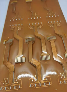
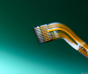
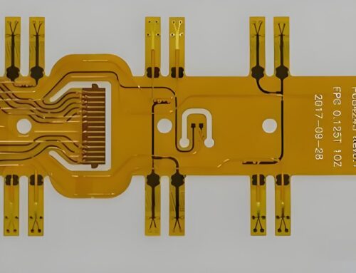
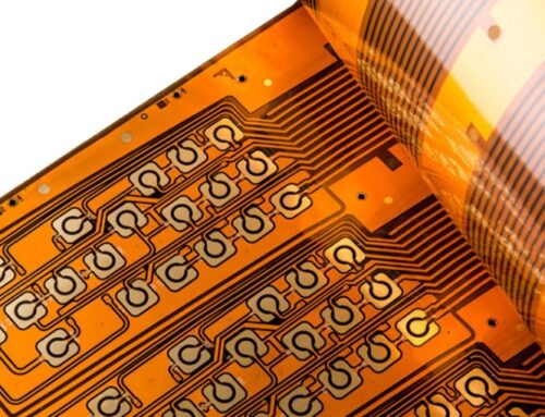
Flexible Printed Circuit (FPC) boards are integral to modern electronics due to their flexibility, lightweight nature, and ability to be tailored to specific applications. Designing an FPC Circuit board requires a comprehensive understanding of its layered structure and careful consideration of layout techniques. This article delves into the design methods and techniques that ensure optimal functionality and reliability in FPC boards, providing a detailed guide for engineers.

Layer Composition of FPC Circuit Boards
An FPC board is typically composed of three main layers: the copper foil layer, the substrate layer, and the silkscreen layer. The copper foil layer encompasses the signal and internal power layers designed in the software, which primarily facilitate the electrical connections in the circuit. The number of copper foil layers is often used to define the type of PCB—whether it’s a single-sided, double-sided, or multi-layer board.
The substrate layer, also known as the insulating layer or copper-clad laminate, serves to isolate the power and routing layers, providing structural support for the entire PCB. The silkscreen layer, positioned on the topmost part of the board, protects the copper foil and carries various markings and symbols (usually in white), aiding in assembly and maintenance.
Key Layout Principles for FPC Circuit Board Design
FPC design largely relies on manual layout, following these critical guidelines:
Functional Layout Based on Circuit Diagram
Components should be arranged as closely as possible to the schematic, ensuring that signals flow smoothly from the left side to the right side or from the top to the bottom. Position each functional circuit unit strategically to maintain consistent signal directionality and flow.
Core Circuit-Centered Layout
Arrange components uniformly, neatly, and compactly. Separate the layout of digital and analog circuits to minimize interference.
High-Frequency Component Connections
Keep connections between high-frequency components as short as possible to reduce electromagnetic interference. Components that are susceptible to interference should be distanced appropriately, and those with high potential differences must comply with safety regulations.
Placement of Adjustable Components
Place adjustable components in easily accessible locations on the PCB. If external adjustments are needed, ensure that their positions correspond to the adjustment knobs on the device’s panel. Components should be at least 3mm away from the edge of the PCB. Heavy components should not be mounted on the PCB, and heat-sensitive components should be placed away from heat-generating parts.
Component Placement Order
Begin with fixed-position components that closely integrate with the structure, such as power sockets, indicators, switches, and connectors. Next, place special components like heat-generating parts, transformers, and ICs. Finally, arrange smaller components like resistors, capacitors, and diodes.

Types of FPC Circuit Boards
FPC boards are generally categorized into the following types:
Single-Sided FPC
The simplest and most cost-effective type, ideal for applications with low electrical performance requirements. It features a single layer of chemically etched conductive patterns on a flexible insulating substrate, typically made of materials like polyimide, polyester, aramid fiber ester, or PVC.
Double-Sided FPC
It consists of conductive patterns etched on both sides of an insulating film, connected by metalized vias to form conductive paths. The covering film protects the conductive traces and indicates component placement. This design caters to both flexibility and functional demands.
Multi-Layer FPC
Multiple layers (three or more) of single or double-sided FPCs are laminated together, with vias and plated through-holes forming inter-layer conductive paths. This structure offers higher reliability, better thermal conductivity, and ease of assembly. Designers must carefully consider the trade-offs between flexibility, layer count, and installation dimensions.
Rigid-Flex PCBs
Traditional rigid-flex boards combine rigid and flexible substrates selectively laminated together, connected by metalized vias. Ideal for designs where components are on both sides of the board, although dual-sided FPCs with FR4 reinforcement on the backside can be a more economical option when all components are on one side.
FPC Board Routing Techniques
Conductive Traces
– Width
The minimum width of conductive traces is determined by their adhesion strength to the substrate and the amount of current they carry. Wherever possible, especially for power and ground lines, traces should be as wide as the layout permits. Even under space constraints, the trace width should not fall below 1mm. This is particularly crucial for ground lines to reduce the overall resistance of the ground system. For traces longer than 80mm, even with low current, the width should be increased to minimize voltage drops affecting circuit performance.
– Length
Minimizing trace length is essential to reduce interference, crosstalk, and parasitic inductance, thereby lowering radiation. This is especially important for the gates of field-effect transistors (FETs), transistor bases, and high-frequency circuits.
– Spacing
The spacing between adjacent traces must meet electrical safety standards. Crosstalk and voltage breakdown are the primary electrical characteristics affecting spacing. To ensure ease of operation and production, spacing should be as wide as possible, with the minimum distance tailored to the applied voltage, including operating voltage, transient fluctuations, and peak voltages caused by other factors. When mains voltage is present, spacing should be even wider for safety.
– Path
The width of signal paths should be consistent from the driver to the load. Changes in path width can alter the impedance, causing reflections and unbalanced circuit impedance. Therefore, maintaining a uniform path width is recommended. Right angles and sharp angles should be avoided in routing; corners should exceed 90° as sharp angles can generate concentrated electric fields, causing noise coupling to adjacent paths. A 45° path is preferable to right or sharp angles. When two traces meet at a sharp angle, the angle should be rounded.

Hole Diameter and Pad Size
The diameter of component mounting holes should closely match the lead diameter, with the hole diameter being slightly larger (by 0.15–0.3mm). For DIL package pins and most small components, a 0.8mm hole diameter with a 2mm pad diameter is standard. For larger holes, the pad diameter should be adjusted accordingly to ensure strong adhesion. Pad-to-hole diameter ratio is about 2:1 for epoxy glass substrates and 2.5–3:1 for phenolic paper substrates.
Conclusion
Designing an FPC circuit board requires ensuring components function effectively within flexibility, space, and electrical performance constraints. Following these design principles, engineers can optimize FPC board performance and reliability for advanced electronic applications.


Leave A Comment