High-Frequency Flexible PCB Impedance Control: Complete Design & Engineering Guide
1. Introduction
Why the high frequency flexible PCB broken by wrong derating? It’s a question often asked by RF engineers. In the case of high frequency boards such as those used in 5G, IoT modules, and aerospace systems, small impedance mismatches can lead to large signal reflections, which in turn degrade the signal integrity of the system as a whole.
What is a High Frequency PCB?
Introduction: High frequency PCB is a circuit board designed for high frequency signals. It works at frequencies of 500MHz or higher, even reaching GHz. Engineers extensively use such boards in high frequency applications, including wireless telecommunication systems, radar systems, satellite electronics, and high-speed digital circuits.
Made with materials that have low loss and low dielectric constant. This helps reduce signal loss and provides stable transmission over a wide frequency range.
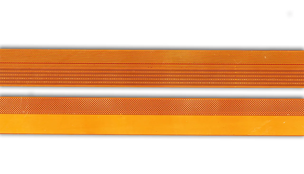
High-Frequency Flexible PCBs, or HF PCBs, work from hundreds of MHz to several GHz. They are important for keeping the design intent. The structure and materials of flexible PCBs make impedance control harder than with traditional rigid boards. These are even more evident in high-frequency PCB design, where accurate signal transmission and impedance matching are vital.
2. Basics of Impedance Control in Flexible PCBs
2.1 What is Characteristic Impedance?
Characteristic impedance measures how much a transmission line resists AC electricity (alternating current). It is a function of the geometry of the conducting path and the dielectric properties of the surrounding materials.
At high frequencies, we need to control this impedance to match the system impedance. This is usually 50 or 100 Ohms. Doing this prevents signal reflection and impedance mismatches. Effective impedance matching is particularly vital in high speed design applications to avoid degradation in performance.
There are microstrip and stripline configurations in flexible PCBs. But owing to bending or additional deformation, impedance consistency becomes more complicated for a flexible substrate than a rigid one.
2.2 Flexible vs Rigid PCB Impedance Behavior
| Attribute | Flexible PCB | Rigid PCB |
|---|---|---|
| Mechanical Behavior | Bends and flexes | Stiff, stable |
| Impedance Stability | Affected by bending and thermal cycling | More consistent |
| Material Movement | Possible under strain | Minimal |
| Use Case Sensitivity | Critical for wearable and mobile RF applications | Suitable for fixed high-speed infrastructure |
In flexible circuits, the impedance can change in time due to bending, temperature changes, and differences in adherence. This complicates the management of real-time signal integrity and long-term stability.
3. Key Factors Affecting Impedance
Understanding what impacts impedance is crucial when working with high-frequency flexible PCBs. The following sections break down three major factors, each playing a role in determining impedance values and overall signal behavior. Each of these is fundamental in ensuring consistent signal transmission and minimizing noise.
3.1 Material Selection
Choosing the right materials is foundational. The dielectric constant (Dk) and dissipation factor (Df) directly influence signal propagation and losses:
| Material Type | Dielectric Constant (Dk) | Dissipation Factor (Df) | High Frequency Suitability |
| Polyimide (PI) | 3.5–3.8 | ~0.008 | Good thermal stability, but moderate loss |
| Liquid Crystal Polymer (LCP) | ~3.0 | ~0.002 | Excellent signal integrity, low loss |
| PTFE | 2.2–2.6 | ~0.001 | Best for ultra-high frequency boards |
Low Dk and Df values reduce signal loss. They are important for high-frequency uses like radar, millimeter-wave communication, and fast wireless systems.
Copper foil type is another important consideration. Rolled annealed (RA) copper has smoother surfaces than electro-deposited (ED) copper. This helps reduce skin-effect losses in high-frequency circuits.
3.2 Stackup Design
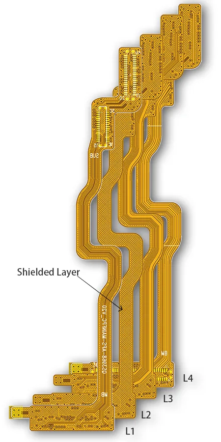
Stackup design determines the physical spacing between conducting layers and dielectric materials, which directly controls impedance and signal behavior. Key factors include:
- Dielectric layer uniformity: Variations affect consistent impedance.
- Signal-to-ground spacing: Closer distance reduces loop area, minimizing EMI.
- Layer count: Higher counts allow embedded stripline routing and shielded paths.
Here’s a quick comparison of flex stackups:
| Stackup Type | Layer Count | Application | Notes |
| Microstrip (2-layer) | 2 | Simple RF traces | Signal above solid ground |
| Embedded Stripline | 3–4 | Noise-sensitive signals | Sandwiched between grounds |
| Shielded Flex | 4–6 | EMI-sensitive circuits | Uses copper shields, adds complexity |
3.3 Trace Geometry
The shape and dimensions of traces heavily affect impedance. Specifically:
Trace Width and Impedance Relationship
The width of a PCB trace directly affects its impedance—narrower traces result in higher impedance, whereas wider traces lower it. To maintain consistent impedance, it’s critical to keep trace width variations within a ±20% tolerance. Achieving this requires compensating for manufacturing discrepancies such as etch undercut, lithography deviations, and pattern transfer inaccuracies during photomask engineering.For high-frequency signal integrity, designers must carefully select trace dimensions and stackup configurations to meet target impedance values within specified tolerances. Modern ECAD tools streamline this process by automating impedance calculations.
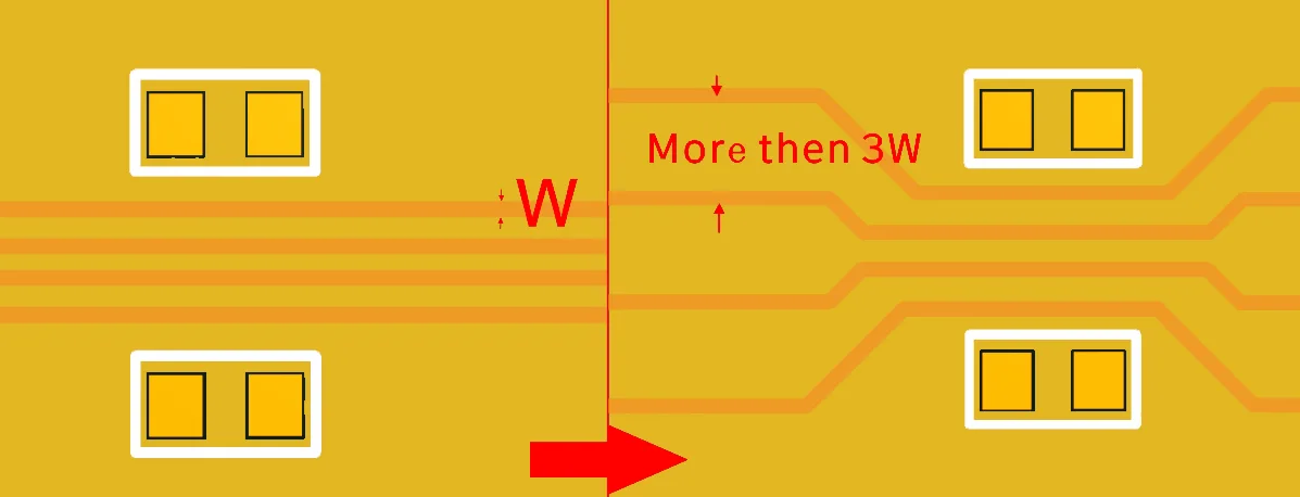
Signal Trace Spacing Best Practices

To minimize crosstalk and interference in high-speed designs:Increase Spacing Between Adjacent Traces – Maintain a minimum clearance of 3W(where W = trace width) between parallel signal lines.
Reduce Parallel Run Lengths – Limit the length of closely spaced parallel traces to decrease capacitive coupling.
Prioritize Critical Signals – Apply stricter spacing rules (e.g., ≥5W) for sensitive high-frequency or differential pairs.
Impact of Copper Trace Thickness and Roughness on Impedance
The thickness of copper traces plays a critical role in determining impedance—thicker copper layers reduce impedance, while thinner layers increase it.Additionally, copper surface roughness can influence high-frequency signal performance, making it another key factor in impedance management.Minimizing Vias for Signal Integrity
Vias introduce parasitic effects that can degrade signal performance:Each via contributes approximately 0.5 pF of distributed capacitance, potentially slowing signal propagation.
Excessive vias increase the risk of data errors and impedance discontinuities, especially from via stubs.
Designers typically use impedance calculators or electromagnetic solvers to fine-tune trace geometry. A simplified formula for microstrip impedance:
Z₀ ≈ (87 / √Dk) × log₁₀(5.98H / (0.8W + T))
Where:
- Z₀ = characteristic impedance (ohms)
- H = dielectric height
- W = trace width
- T = copper thickness
4. Design Techniques for Impedance Control
Precision in layout and simulation helps engineers achieve target impedance values reliably. Below are practical methods to ensure consistent performance.
4.1 Accurate Simulation and Modeling
Instead of relying on theoretical calculations alone, simulation software helps model realistic behavior. Recommended tools include:
- Polar SI9000: Widely used for controlled impedance stackup planning.
- Keysight ADS: Useful for system-level signal integrity analysis.
- ANSYS HFSS: Ideal for complex RF simulations and 3D modeling.
Important considerations:
- Input accurate Dk/Df values matching operational frequency ranges.
- Account for manufacturing tolerances.
- Simulate full interconnect paths, including vias and transitions.
4.2 Bending Area Compensation
Flex circuits introduce unique challenges when signals pass through dynamic regions. Design tips:
- Avoid 90° bends; use gradual arcs to preserve the signal waveform.
- Use stiffeners to support areas with impedance-critical traces.
- Enlarge the bend radius in RF zones to reduce mechanical stress.
4.3 Grounding and Shielding Strategy
A robust ground structure minimizes EMI, reflections, and signal distortion. Consider the following approaches:
| Ground Type | Benefits | Drawbacks |
| Solid Ground Plane | Best signal return path, stable impedance | May increase overall stiffness |
| Grid Ground | Lighter, more flexible | Risk of impedance fluctuation at high frequencies |
| Shielding Layer | Effective for EMI-sensitive lines | Adds cost and thickness |
Use ground stitching vias liberally and maintain consistent reference planes across signal layers. For differential signals, symmetry and coupling are vital to preserve impedance.
5. Manufacturing and Testing Challenges
5.1 Manufacturing Tolerance Control
Achieving ±10% impedance tolerance is considered good in flexible PCB manufacturing. However, flex circuits introduce complexities such as:
- Variations in dielectric thickness due to adhesive squeeze-out.
- Etching inaccuracies during trace definition.
Experienced PCB manufacturers specializing in flexible PCBs are crucial for high-frequency boards.
5.2 Impedance Testing Methods
Two common impedance validation tools:
- TDR (Time-Domain Reflectometer): Fast, reliable, used during production.
- VNA (Vector Network Analyzer): More advanced, accurate across frequency ranges.
Testing coupons should mimic actual stackup and routing conditions.
6. High-Speed vs High-Frequency Flexible PCBs
While often used interchangeably, high-speed data (measured in Gbps) and high-frequency signal (measured in GHz) are not the same:
| Comparison Point | High-Speed Flexible PCB | High-Frequency Flexible PCB |
| Concern | Data rate (Gbps) | Signal frequency (GHz) |
| Key Design Focus | Rise/fall time control | Wave propagation & Dk/Df optimization |
| Tools Used | Time-domain simulation | Frequency-domain modeling |
| Typical Application | USB, HDMI, DDR interfaces | RF modules, 5G antennas, Wi-Fi circuits |
Both demand impedance control, but frequency-based designs require greater emphasis on dielectric constant and advanced materials.
7. Case Study: 5G Flexible Antenna PCB
A flex PCB used in a 5G antenna was designed using LCP to support 28 GHz operation. Challenges included achieving 50-ohm impedance in a 3-layer stackup. Using simulation tools and low-Dk adhesive layers, the final design minimized signal loss and passed VNA tests with <5% deviation from the target.
Outcome: Improved high-frequency performance, consistent return loss across the band.
8. Frequently Asked Questions (FAQ)
Q1: What’s the typical impedance for high-frequency flexible PCBs?
A: Typically 50 ohms for single-ended and 100 ohms for differential pairs.
Q2: Can I use polyimide for high-frequency applications?
A: Yes, but LCP is preferred when minimizing loss is critical.
Q3: What causes impedance mismatch?
A: Variations in trace width, dielectric thickness, or material Dk values.
Q4: Do I need simulation software for every design?
A: For high-frequency PCBs, accurate simulation is highly recommended.
Q5: What materials are best for high-frequency signal routing?
A: LCP, PTFE, and other low-loss advanced materials.
9. Conclusion
For a flexible PCB for high frequency, impedance control is a must. From choosing the right materials with constant and stable dielectric properties, to designing for an accurate stackup and trace, all the details matter when it comes to high-speed performance and signal integrity. Whether you are developing flex PCBs for high-frequency applications, RF assemblies, or wearables communication subsystems, focusing on impedance control can significantly contribute to your success.
High Frequency Bill of Materials – Design vs Reality To win at high frequency, the engineer must juggle electrical design with the realities of flexible PCB manufacture. Get primed for your next high-frequency design! Contact our experts to build trustworthy, impedance-controlled flex PCBs.


Leave A Comment