Mastering SMT Assembly: Advantages and Future Trends
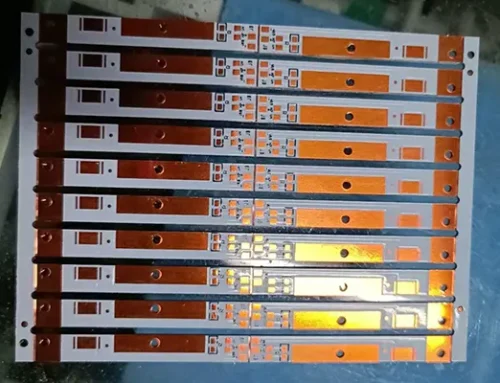
SMT assembly, or Surface Mount Technology (SMT) assembly, is now a key component of the rapidly evolving electronics industry. It has grown with the rise of modern circuit boards. Mobile phones and factory automation equipment use SMT technology. It offers high-density assembly and other benefits for PCB production.
In this guide, we will explore the basics of SMT PCB assembly. We will discuss what it means for SMDs. We will cover everything involved in SMT assembly. This includes solder paste inspection (SPI) and reflow soldering ovens.
What Is SMT Assembly?

SMT Process (Surface Mount Technology): Surface Mount Technology, or SMT, is a manufacturing method used in the electronics industry. Unlike insertion mount components, SMT does not create holes in the PCB. It also does not require anyone to drill lead holes. This allows for 2-3 times more component density on the board.
The SMT manufacturing process typically involves:
Solder paste printing using a stencil
Component placement with pick and place machines
Reflow soldering in a reflow soldering oven
Inspection (SPI and AOI)
Functional and in-circuit testing
This end-to-end automated PCB assembly is enabling greater consistency, lower labor cost, and higher throughput.
What Is the Difference Between SMT and SMD?
One common misconception in electronics manufacturing is the distinction between SMT and SMD.
- SMT stands for Surface Mount Technology. It is the process used for manufacturing. THT stands for Through Hole Technology, which is an older type of manufacturing method. It is a comprehensive method for placing and soldering parts directly to the board surface simultaneously with reflow soldering.
- SMD stands for Surface Mount Device. It is the general name for the components used in SMT. SMDs are actually resistors, capacitors, diodes, integrated circuits, and the like. Such components are generally leadless or have very short leads, making them suitable for high-density applications.
In simple terms:
SMT is the process. SMD is the component.
SMT Assembly Process Explained
The SMT PCB assembly process is a series of automated steps that ensure high precision and speed:
1. Solder Paste Application
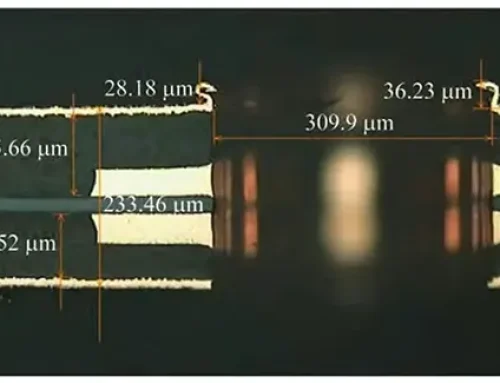
A solder paste printer places solder paste on the pads of the PCB. The paste is a combination of molten solder balls and flux, which is essential for reliable solder joints.
2. Solder Paste Inspection (SPI)
Automated SPI machines scan the board to verify paste volume and alignment. Accurate SPI minimizes solder joint defects and enhances yield.
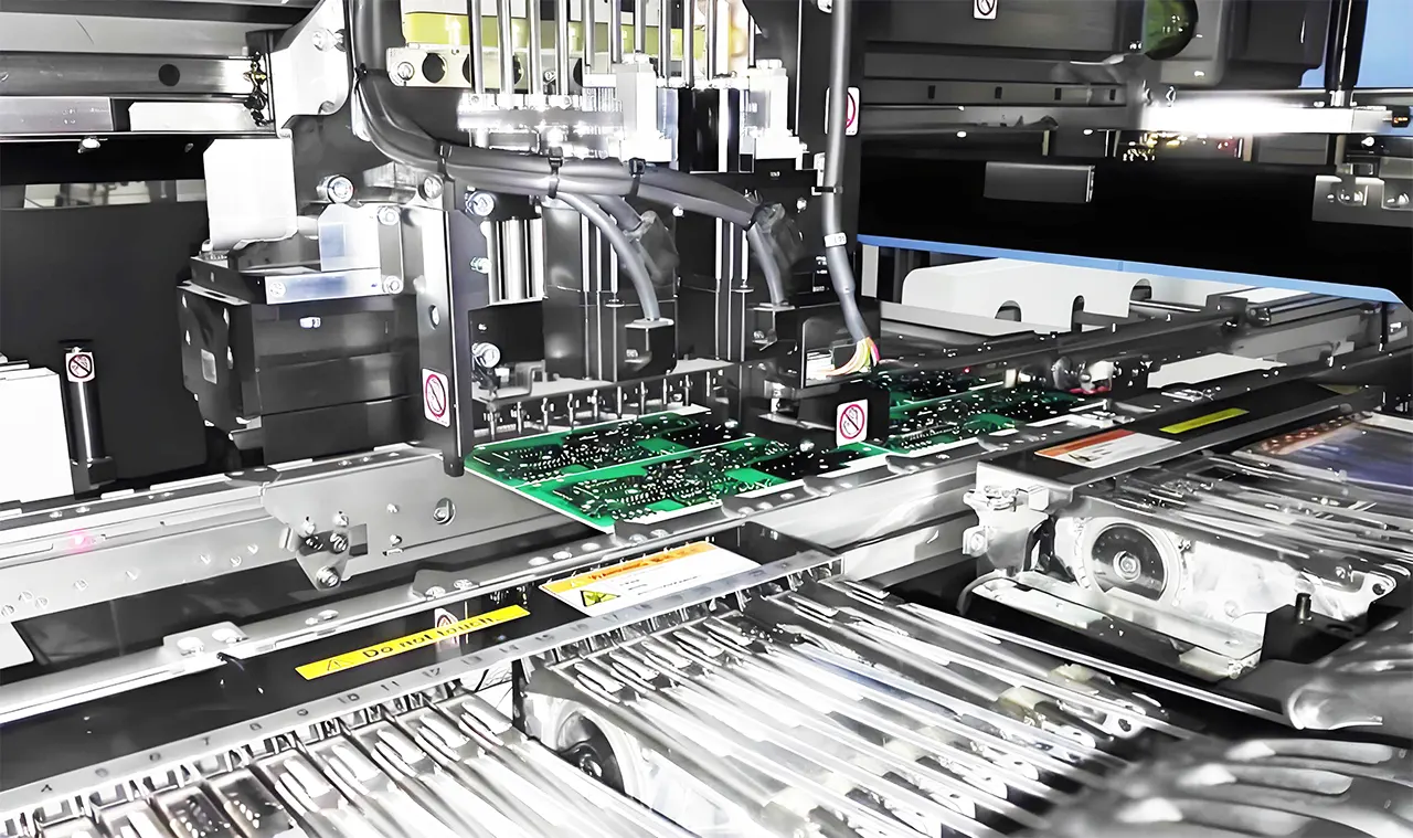
3. Pick and Place
High-speed pick and place machines precisely position SMD components onto the paste-covered pads, based on the board design.
4. Reflow Soldering
Beim Bestücken von Leiterplatten wird die Platine in einen Reflow-Lötofen geschoben. Dort werden die Lötstellen durch Temperaturzonen verflüssigt. So werden die Bauteile mit der Oberfläche der Leiterplatte verbunden.
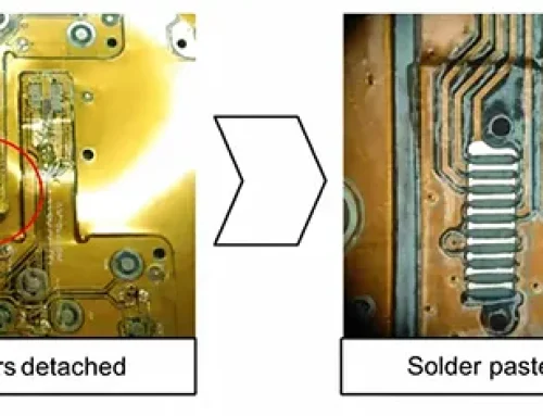
5. Automatic Optical Inspection (AOI)
After soldering, AOI checks that components are in the right position and soldered correctly. This helps find problems early in production.
6. Testing
After soldering, AOI checks that components are in the right position and soldered correctly. This helps find problems early in production.
Advantages of SMT Assembly
The advantages of SMT over traditional hole technology (through-hole assembly) are significant:
- High component density: SMT enables double-sided SMT assembly, allowing components on both sides of the PCB.
- Smaller form factor: Eliminates the need for drilling holes for hole components or long component leads.
- Automation-friendly: Supports full-scale SMT assembly line automation for higher consistency and speed.
- Reduced cost: Less manual labor, smaller boards, and an efficient assembly process result in lower overall costs.
- Improved performance: Shorter electrical paths reduce signal delay and improve RF performance.
These benefits make advanced SMT assembly the default for most PCB manufacturing operations today.
Disadvantages of Surface Mount Technology
Despite its benefits, surface mount technology SMT does have limitations:
- Heat sensitivity: High heat can damage small components and SMDs if they are not set correctly in the reflow oven.
Mechanical strength: SMT components are not as mechanically robust as through-hole counterparts.
Inspection complexity: Miniaturized SMT components make visual or manual inspection difficult without sophisticated equipment.
For high-power or mechanically stressed applications, engineers may still prefer hole components.
SMT vs Through-Hole Components (Hole Technology)
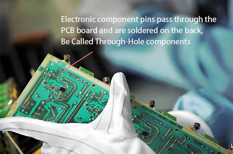
SMT and through-hole (also known as hole technology) serve different roles in circuit board assembly:
| Aspect | SMT | Through-Hole components (Hole Technology) |
|---|---|---|
| Mounting Method | Surface-mounted | Inserted into holes |
| Assembly Type | Automated | Often manual |
| Component Type | Surface mount device (SMD) | Hole components |
| Density | High | Low |
In many cases, a circuit board has two sides. One side uses SMT, and the other uses hole technology. This design helps balance density and durability.
Uses for Surface Mount Technology
Surface mount assembly is essential across a wide range of industries:
Consumer Electronics: Phones, laptops, smartwatches
Medical Devices: Portable monitors, wearable sensors
Automotive: Engine control units, infotainment systems
Aerospace: Flight control systems, navigation modules
Industrial Controls: PLCs, sensors, robotics
Its ability to handle miniaturized electronic components makes SMT ideal for high-volume, compact product manufacturing.
Take Your Design Into the Future
The following are some expert insights to help you maximize your next SMT board assembly:
DFM: Collaborate with your board house to make sure that the design matches SMT.
Components arrangement: placement according to IPC, space, direction, and solder mask to comply with the requirements.
Test points: Integrate accessible test pads to support quality control and maintenance.
Double-sided design: Evaluate whether a double-sided circuit board assembly can reduce space and cost.
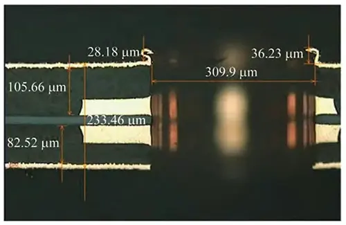
When designing for advanced SMT assembly, every micron counts. Compact layouts, smart placement, and process-aware design can reduce costs, improve quality, and shorten production cycles.
Conclusion
PCB Board Assemblies
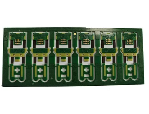
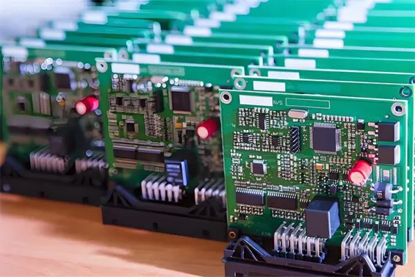
SMT assembly continues to redefine the standards of printed circuit board (PCB) production. It is the gold standard for doing today’s high-volume, high-performance, miniaturized electronics.”
Engineers and procurement experts can improve product performance. They can do this by understanding the differences between SMT and SMD. Additionally, enhancing the SMT build process is important.
Learning the basics of SMT can help you in PCB assembly. It can also enhance SMT assembly machines and circuit board assembly, regardless of the task at hand. You may also want to explore our capabilities in Flex PCB Assembly — ideal for flexible designs and dynamic applications.