
Flexible PCB Failure Modes: Causes, Prevention, and Design Best Practices

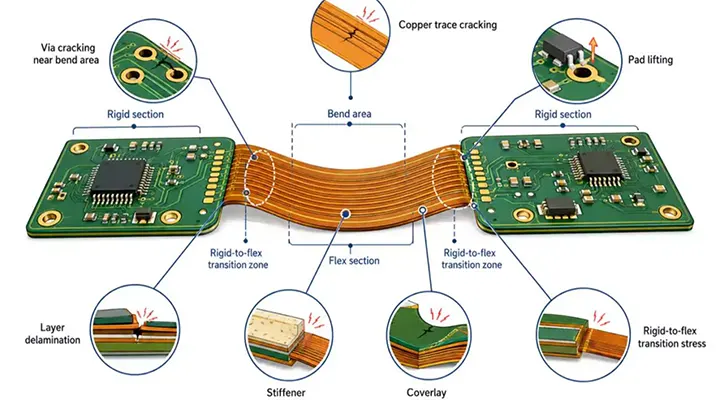
Flexible printed circuit boards (FPCBs) have become indispensable in modern electronics because they reduce weight, save space, and enable three-dimensional packaging. Consumer electronics, automotive, aerospace, industrial automation, and medical devices increasingly rely on flexible circuits to improve reliability while accommodating complex mechanical designs. Yet flexible PCB failure causes differ sharply from those of rigid boards: flex circuits undergo continuous bending, twisting, vibration, and thermal cycling in service, so mechanical factors overlooked during development can cause even a well-manufactured circuit to fail prematurely. IPC-2223, the Design Standard for Flexible Printed Boards, indicates that most flex-circuit failures originate from mechanical stress concentration rather than electrical defects, and studies from NASA and IPC show that material selection, bend-radius control, and component placement strongly influence long-term reliability. This article examines the most common flexible PCB failure modes, explains why they occur, and outlines engineering practices that reduce failure risk.
Key Takeaways
- Flexible PCB failures usually start as mechanical strain concentration in copper, vias, coverlay, or solder joints, not as electrical defects.
- Separate static bend zones from dynamic bend zones. Dynamic zones need RA copper, larger bend radius, and no vias or pads.
- Use quantified starting points: dynamic bend radius about 10× total thickness, static bend radius about 1–2× total thickness, and traces crossing the bend line at 90°.
- Keep vias, pads, and plated through holes out of bend zones; route a smooth trace through the flexing area instead.
- Use a DFM review checklist and a prevention checklist before release, then confirm with bend fatigue and adhesion tests per IPC-2223 and IPC-6013.
- Do not mix manufacturing-era defects with field fatigue failures; the timing, evidence, and corrective actions are different.
Why Flexible PCBs Fail
Meanwhile, unlike rigid boards, a flexible circuit keeps deforming while it carries current. For example, every bend cycle pushes tensile and compressive stress into the copper, the dielectric film, the vias, and the solder joints. In addition, the IPC-2223 Design Standard for Flexible Printed Boards notes that most flex circuit failures come from mechanical stress concentration rather than electrical defects. As a result, studies published by NASA and the IPC point the same way: material selection, bend-radius control, and component placement drive long-term reliability.
In practice, these failures are also hard to diagnose. Next, the stack is thin and often multilayer; there is no rigid support to hold a shape, and damage accumulates over thousands of cycles. A crack that finally opens a circuit usually started as a microscopic defect months earlier. That is why flexible circuit boards tend to fail gradually instead of all at once.
Consequently, the main causes of flexible PCB failure are summarized below.
| Failure driver | Effect on the flexible PCB |
|---|---|
| Excessive bending | Copper fatigue and conductor cracking |
| Small bend radius | High localized mechanical strain |
| Thermal cycling | Expansion mismatch between materials |
| Vibration | Progressive fatigue around solder joints and vias |
| Moisture absorption | Delamination and blistering during reflow |
| Improper component placement | Stress concentration and pad lifting |
| Poor material selection | Reduced flex life and premature cracking |
Moreover, small defects grow under repeated mechanical loading. Therefore, the purpose of a design review is to lower strain early, not to inspect harder at the end of the line.
Manufacturing-Era Defects vs Field Fatigue Failures
In particular, two failure classes get mixed together in troubleshooting. However, manufacturing-era defects appear at first article, reflow, assembly, or incoming inspection: plating voids, laminate voids, contamination, poor adhesion, moisture pickup, and handling damage. Therefore, field fatigue failures appear after repeated bending, vibration, or thermal cycling: copper fatigue, via barrel cracks, coverlay cracking, and progressive pad lift. Additionally, the evidence and the corrective action are different, so separate them before changing the design.
| Question | Manufacturing-era defect | Field fatigue failure |
|---|---|---|
| When it appears | First article, reflow, assembly, or incoming inspection | After repeated bending, vibration, or thermal cycling |
| Typical causes | Plating voids, laminate voids, moisture, contamination, poor adhesion, handling damage | Bend radius too small, vias in bend zone, ED copper in dynamic zone, stress concentration |
| Evidence | Blisters after reflow, peeling, voids in cross-section, adhesion failure | Progressive resistance drift, micro-cracks, barrel cracks, coverlay cracks |
| Prevention | Supplier qualification, bake and dry, cleanliness, first-article cross-section | Design rules, RA copper, bend fatigue test, strain relief |
Copper Trace Cracking and FPC Copper Cracking Prevention
Meanwhile, copper trace fatigue is the most frequently reported failure mechanism in dynamic flex applications. For example, each bending cycle stretches the copper on one side of the neutral axis and compresses the other side. In addition, when the bend radius is too small, plastic deformation builds up inside the copper grains. As a result, micro-cracks then form and grow until the conductor opens.
In practice, most of these failures trace back to a few design choices: bend-radius violations, sharp corners in trace routing, excessive copper thickness, and traces that cross the bend line at a shallow angle. Next, copper type matters as well. Consequently, electrodeposited (ED) copper is widely used, but rolled annealed (RA) copper has a grain structure aligned with the rolling direction. As a result, RA copper tolerates significantly more bending cycles than ED copper.
FPC copper cracking prevention comes down to five rules:
- Keep the bend radius as large as the enclosure allows.
- Specify RA copper for every zone that flexes in service.
- Split a wide conductor into several thin traces, so strain spreads out.
- Hold copper and plating thickness at the minimum that still carries the current.
- Cross the bend line at 90° where possible, and never route a trace parallel to the bend line in a dynamic zone.
Also use teardrops where traces enter a pad, and avoid abrupt width changes. For high-cycle designs, ask the Flexible Circuits supplier to confirm the copper type on the drawing, not only in the quotation.
Via Barrel Cracking and Interconnect Fatigue
A via barrel is a thin plated cylinder, and it sits far from the neutral axis in most stacks. Bending and vibration therefore put the highest strain on the plating. Cracks usually start at the barrel-to-pad junction and grow around the circumference. Once that ring opens, the connection turns intermittent before it fails completely.
Vias belong outside bend zones. Place them in a low-stress area, and let a smooth trace carry the signal through the flexing section. If a via is unavoidable, lower the local strain with a larger pad, a shorter barrel, and a stiffer stack around it. Interconnect fatigue also appears at connector tails and at the rigid-to-flex transition, where stiffness changes abruptly.
Case Example: Dynamic Hinge Interconnect Degradation
A representative wearable hinge design used a 2 mm dynamic bend radius and placed vias in the bend zone near the rigid-to-flex transition. After about 20,000 open-close cycles, resistance rose from 0.9 Ω to 1.8 Ω and then became intermittent. Cross-section showed barrel cracks at the pad junction. The redesign moved vias 3 mm outside the bend, switched the dynamic zone to RA copper, increased the radius to 4 mm, and added strain relief at the connector tail. The revised flex passed 100,000 cycles with less than 5% resistance drift. This case shows how dynamic activity degrades an interconnect long before a visible open appears.
Delamination, Blistering, and Coverlay Cracking
Delamination and blistering are interface failures. Moisture absorbed into the adhesive or the dielectric expands during reflow and separates the layers. Thermal cycling adds a second driver, because the materials in the stack expand at different rates. Nickel–copper adhesion failure follows a similar path at the metal interface, and both problems appear first as haze, bubbles, or lifted film.
Coverlay cracking is the protective-film version of the same story. The coverlay is stiffer than the base film, so cracks start at openings, at bend lines, and where adhesive squeezes out. Once a crack reaches the copper, moisture and flux residue enter the bend zone. In addition, a cracked coverlay hides the copper damage underneath, which slows diagnosis.
Prevention starts with material handling. Keep panels dry, follow the laminate supplier’s bake schedule before lamination, and select an adhesive system that matches the reflow profile.
Solder Joint and Pad Failure
Improper component placement concentrates stress. A stiff component mounted on a bend line will lift its pad, and the solder fillet cracks soon after. Vibration then finishes the job. Pad lifting is common on flex, because the bond between copper and base film is the only thing holding the pad down.
Keep components off bend zones and off the rigid-to-flex transition. Use a stiffener under any part that must sit on flex, and anchor pads with a coverlay opening instead of a free edge. A Flexible PCB that carries a connector at the edge also needs strain relief, so cable movement never reaches the solder tails.
Matching Failure Modes to Inspection Methods
Diagnosis is faster when each symptom maps to one test. The table below links common flexible PCB failure modes to the evidence they leave behind.
| Failure mode | What to look for | Typical inspection |
|---|---|---|
| Copper trace cracking | Micro-cracks across copper grains | Microscope, cross-section, bend fatigue test with continuity monitoring |
| Via barrel cracking | Ring cracks in the plated barrel | Cross-section, resistance and continuity monitoring |
| Delamination and blistering | Haze, bubbles, lifted film after reflow | Visual check, microscope, peel test |
| Solder joint and pad lift | Fillet cracks, peeling pads | AOI, cross-section |
| Coverlay cracking | Cracks at openings and bend lines | Visual check, microscope |
Residue left after cleaning PCB boards can also mask fine cracks under magnification, so always inspect a clean sample. Record the pull test, the cross-section, and the continuity log together. Otherwise, a single photograph proves very little.
Reliability Testing and Acceptance Criteria
Use IPC-2223 for design guidance and IPC-6013 for qualification and performance requirements of flexible printed boards. A practical bend-zone test plan includes bend fatigue with continuous continuity and resistance monitoring, peel or pull testing for adhesion, reflow simulation for moisture and thermal stress, and visual or microscope inspection of coverlay openings after cycling. Acceptance criteria should be written before testing: no continuity interruption, resistance drift within the agreed limit (often ≤10%), no delamination or blistering, no coverlay crack reaching copper, and no barrel cracks in cross-section. Confirm the exact test method and limit with the fabricator and the end customer’s reliability plan.
Quantifiable Design Parameters for Bend Zones
The parameters below turn the failure modes into starting points for the drawing. They are starting points, not universal limits; confirm the final values with the fabricator and a bend fatigue test.
| Parameter | Static bend zone | Dynamic bend zone |
|---|---|---|
| Minimum bend radius | 1–2× total finished thickness as a starting point | 10× total finished thickness as a starting point; verify by bend fatigue test |
| Copper type | ED copper acceptable | RA copper preferred |
| Copper thickness | Use the minimum that carries current | 1/2 oz (17 µm) or thinner where possible |
| Trace orientation | Cross the bend line at 90°; avoid sharp corners | Cross at 90°; no parallel runs in the flexing area |
| Vias and pads | Outside the bend preferred | Not permitted |
| Coverlay openings | Keep off the bend line | Keep off the bend line; ensure adequate adhesive flow |
DFM Review and Prevention Checklist
DFM Review Checklist
- [ ] Mark static and dynamic bend zones on the drawing, with bend direction, radius, and cycle target.
- [ ] Confirm RA copper in every dynamic zone and the thinnest usable copper on the drawing.
- [ ] Check minimum bend radius against the table above and the enclosure envelope.
- [ ] Route traces at 90° to the bend line; remove sharp corners and abrupt width changes.
- [ ] Keep vias, pads, and plated through holes out of bend zones.
- [ ] Keep coverlay openings away from bend lines and confirm adhesive flow.
- [ ] Place components on stiffened areas, never on a bend line or rigid-to-flex transition.
- [ ] Review stack-up balance, adhesive thickness, and material bake requirements.
- [ ] Define bend fatigue, continuity, resistance, and adhesion tests before release.
Prevention Checklist
- [ ] Keep panels dry and follow the laminate supplier’s bake schedule before lamination.
- [ ] Control handling to avoid scratches, dents, and contamination before coverlay.
- [ ] Use teardrops at trace-to-pad entries and split wide conductors into thinner traces.
- [ ] Add strain relief at connector tails and cable exits.
- [ ] Anchor pads with coverlay openings instead of free edges.
- [ ] Inspect a clean first article with cross-section, pull test, and continuity log.
- [ ] Monitor resistance drift during bend fatigue, not only open-circuit failure.
For medical, automotive, and industrial programs, High-Reliability Flexible Circuits for High-End Applications usually need a documented DFM review, a bend fatigue test plan, and a traceable material list. As a Flexible PCB Manufacturer, Gekun builds single-sided, double-sided, multilayer, and rigid-flex parts, reviews bend zones at quotation, and can supply RA copper on request.
Glossary of Flexible PCB Failure Terms
- Coverlay: protective dielectric film laminated over flex circuitry; cracks at openings or bend lines can expose copper.
- Coverlay cracking: a crack in the protective film, often at openings, bend lines, or adhesive squeeze-out; it can hide copper damage underneath.
- Pad lift: separation of a copper pad from the base film, usually from stress concentration, poor adhesion, or a component on a bend line.
- Silver paste through-hole: a printed through-hole connection filled with silver paste; it can crack under bending or thermal cycling, especially in membrane switch and printed flex designs.
- Via barrel: the plated cylinder connecting layers; cracks start at the barrel-to-pad junction under bending or vibration.
- Delamination: separation between layers, often from moisture expansion during reflow or thermal expansion mismatch.
- Blistering: a localized bubble or lifted film after reflow, usually a moisture or adhesion failure.
- Neutral axis: the layer in a bent stack that sees neither tension nor compression; copper placed away from it sees higher strain.
- Dynamic bend zone: an area that flexes repeatedly in service; it needs the strictest design rules.
- RA and ED copper: rolled annealed copper has grains aligned with the rolling direction; electrodeposited copper is common but less tolerant of repeated bending.
FAQ
Can vias be placed in a flex bend area?
No. A via barrel is a plated cylinder, and it carries the highest strain in the stack. Vibration and bending fatigue the plating around the barrel until it cracks. Keep vias, pads, and plated through holes outside the bend zone, and route the connection with a smooth trace instead. If a via is unavoidable in a static bend area, move it as far from the bend line as possible and review the local stack-up.
What dynamic bend radius should I specify?
Use about 10× the total finished thickness as a starting point for a dynamic bend zone, and about 1–2× total thickness for a static bend that is formed during assembly. These are starting points from flex design practice and IPC-2223 guidance, not universal limits. Confirm the final radius with a bend fatigue test at the target cycle count and monitor continuity and resistance.
Does dynamic bending require RA copper instead of ED copper?
Yes, for the flexing zone. Rolled annealed copper has grains aligned with the rolling direction, so it survives far more bending cycles than electrodeposited copper. ED copper is acceptable in static areas that bend only during assembly. IPC-2223 treats this as a design decision, not a purchasing detail.
What causes coverlay cracking in flex circuits?
The coverlay is stiffer than the base film, so cracks start at openings, bend lines, and where adhesive squeezes out. Once a crack reaches the copper, moisture and flux residue enter the bend zone. Prevent it by keeping coverlay openings away from bend lines, controlling adhesive flow, and validating the bend zone with fatigue testing and microscope inspection.
Why do pads lift on flexible PCBs?
Pad lift usually comes from stress concentration. A stiff component mounted on a bend line, a free pad edge, poor copper-to-base-film adhesion, or missing stiffener can all lift the pad. Keep components off bend zones, use a stiffener under parts that must sit on flex, and anchor pads with a coverlay opening instead of a free edge.
What is silver paste through-hole cracking?
In membrane switches and some printed flex designs, a through-hole is filled with silver paste to connect layers. Bending, thermal cycling, or poor fill can crack that paste and raise resistance or open the circuit. Keep silver paste through-holes out of bend zones, control fill quality, and include continuity monitoring in the qualification test.
What is the most common cause of flexible PCB failure?
Mechanical stress concentration. Bend radius violations, vias in bend areas, and stiff components placed on a bend line all focus strain on a small copper area. According to IPC-2223 and NASA/IPC studies, material selection and bend-radius control improve long-term reliability more than any electrical tweak.
How do I tell a manufacturing defect from field fatigue?
Check timing and evidence. Manufacturing-era defects appear at first article, reflow, or assembly as blisters, peeling, voids, or adhesion failures. Field fatigue appears after repeated bending, vibration, or thermal cycling as progressive resistance drift, micro-cracks, barrel cracks, or coverlay cracks. Use cross-sections, pull tests, and continuity logs to separate the two before changing the design.
How do I check FPC copper cracking prevention on a new design?
Run a bend fatigue test on a prototype with continuous continuity and resistance monitoring. Combine it with a cross-section of the bend area to confirm copper grain direction and plating thickness. If resistance drifts before the target cycle count, change the bend radius, copper type, or trace orientation.
Related Posts
- Nickel–copper adhesion failure in flexible PCBs | Causes & Fixes | Gekun — Related article
- Flexible PCB: Features, Design Guide & Applications — Related article
- AI-Driven Optimization of Flexible Circuit Boards Production — Related article
- Cleaning PCB Boards — Related article
- Closed-Loop Recyclable Flexible PCB Manufacturing Guide — Related article