
PCB Lamination Process Explained: From Rigid Boards to Flexible PCB Manufacturing
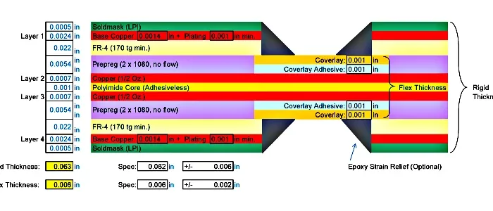
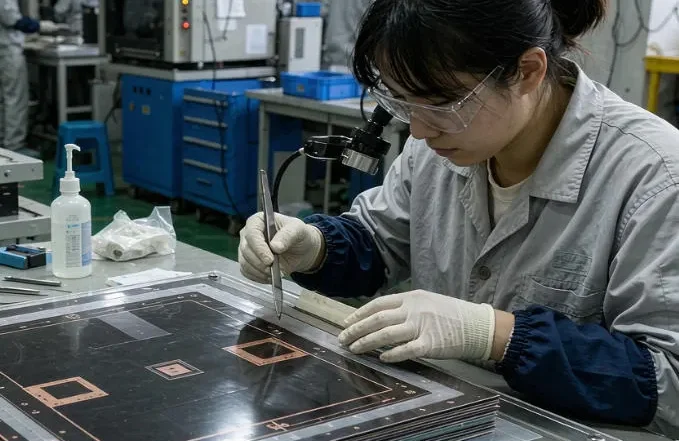
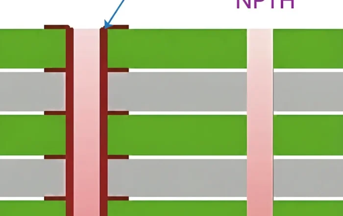
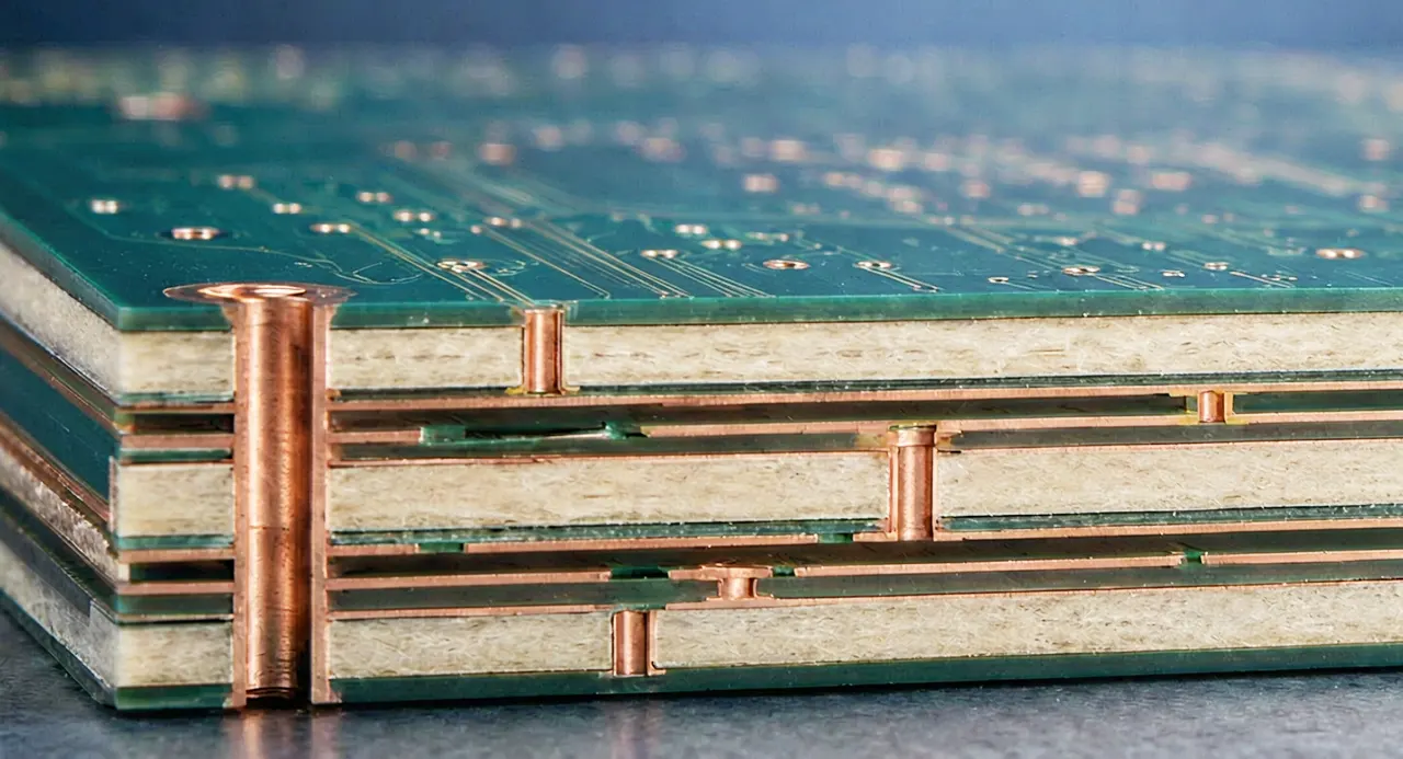
PCB Lamination is the step that bonds copper foil, prepreg or adhesive, and a core or polyimide base into one solid board under heat and pressure. It determines layer adhesion, thermal endurance, and mechanical strength. In addition, it is the core of both rigid and flexible PCB lamination.
For a flex board or a Rigid-Flex PCB, the idea is the same. However, the process window is much tighter. Thin copper and special adhesive layers leave little room for error.
What Is PCB Lamination?
PCB lamination stacks copper and insulating layers, then bonds them at a set temperature and high pressure. The goal is one board with good conductivity and mechanical strength.
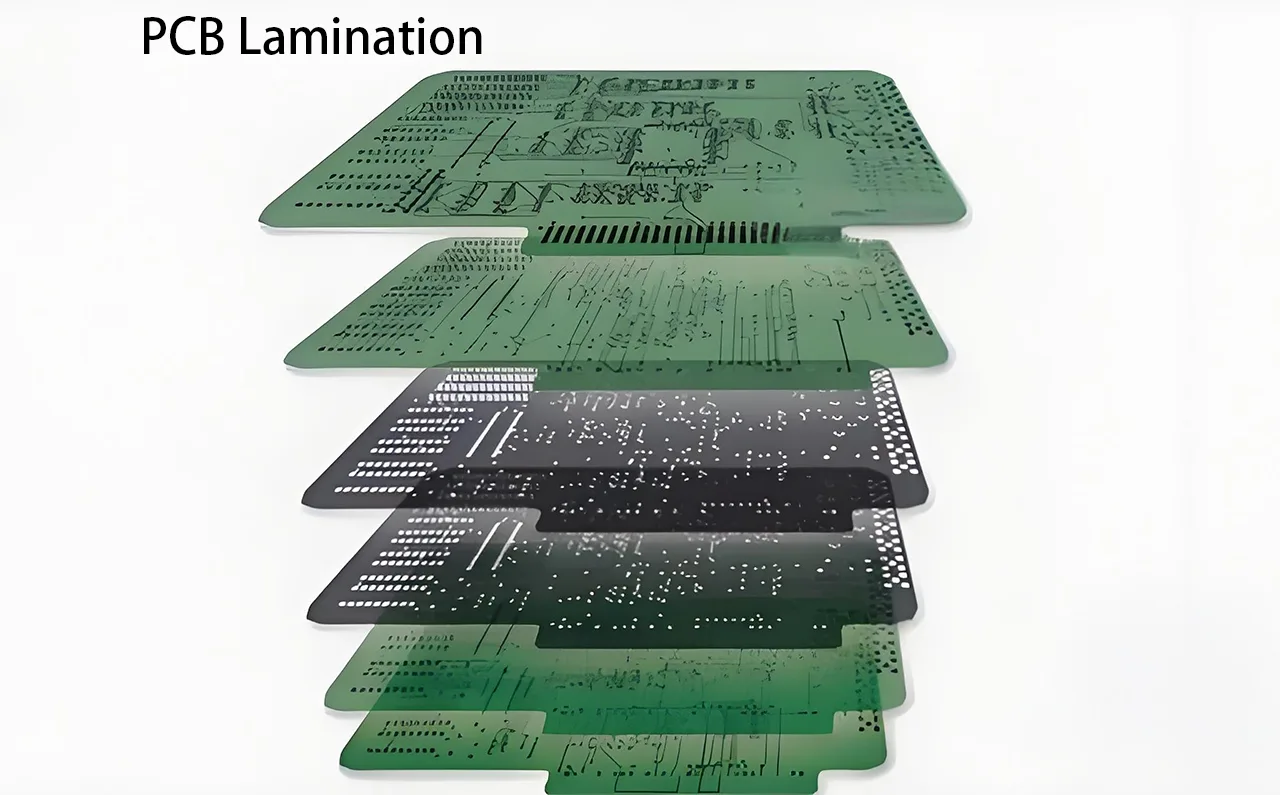
Four material groups do the work:
- Copper foil – the conductive base that becomes circuit traces.
- Prepreg or adhesive layer – the bonding material that holds layers together.
- Core or base film – FR4 for rigid boards, polyimide for a flexible PCB.
- Coverlay or solder mask – protects circuit patterns and provides insulation.
Therefore, lamination is more than stacking. It needs precise alignment, air removal and strong adhesion between every layer.
PCB Lamination Process Steps
Most shops follow the same sequence, from rigid multilayer builds to thin flex circuits.
1. Material preparation. Copper foil, prepreg, core or polyimide film and coverlay are cut to panel size and checked.
2. Lay-up and alignment. Layers enter the stack in the designed order. Tooling pins and targets keep the pattern registered.
3. Air removal. Vacuum pulls trapped air out of the stack. Leftover air turns into voids later.
4. Hot press. Heat and pressure cure the prepreg or adhesive. Multilayer boards may need more than one press cycle.
5. Cooling under pressure. The stack cools while still clamped. This step limits warp and built-in stress.
6. Post-processing. Drilling, plating and surface finish follow, as covered in our etching and copper plating guides.
Four parameters decide the result: temperature, pressure, vacuum level and heat ramp rate. Also, the resin flow of the prepreg must match the copper pattern.
Typical Lamination Curve and Parameter Windows
A typical press cycle follows a repeatable curve: preheat and vacuum, controlled ramp to cure temperature, a cure hold under pressure, then cooling while pressure is still applied. The exact window depends on resin chemistry, copper thickness and stack height. The table below gives typical starting ranges; always confirm with the material datasheet and a press trial.
| Material system | Typical temperature | Typical pressure | Vacuum and ramp | Key notes |
|---|---|---|---|---|
| Rigid FR4 multilayer | 180–200°C | 200–400 psi (1.4–2.8 MPa) | Vacuum <10 mbar; ramp 2–5°C/min | Watch resin flow, warp and prepreg shelf life. |
| Flexible polyimide | 160–180°C | 80–200 psi (0.6–1.4 MPa) | Vacuum <10 mbar; ramp 1–3°C/min | Lower heat and pressure reduce wrinkles and dimensional shift. |
| Rigid-flex | 170–190°C | 150–300 psi (1.0–2.1 MPa) | Vacuum <10 mbar; ramp 1–3°C/min | Use fillers or shims for uneven stacks; protect unbonded flex zones. |
For different material systems, moisture control and ramp rate matter as much as the final hold. Damp polyimide or prepreg can create voids before the resin gels. A slow ramp lets air escape and resin flow evenly. Cooling under pressure is not optional; it locks the stack flat and limits built-in stress.
Types of PCB Lamination
Different circuit designs require different lamination techniques. The most common types include:
1. Standard Rigid PCB Lamination
It is used in both consumer and industrial electronics. It has layers of prepreg pressed with copper foil at high temperature. The result is a solid, long-lasting fabric; however, it is quite rigid.
2. Multilayer PCB Lamination
Here, more than four copper layers are stacked and laminated together. The process involves multiple press cycles, ensuring accurate circuit design alignment and high reliability.
3. High-Density and HDI PCB Lamination
Microvia lamination and sophisticated surface finish processes are necessary in high-density designs. These PCBs are frequently found in smartphones, laptops, and other high-performance electronics.
4. Rigid Flex PCB Lamination
Microvia lamination and sophisticated surface finish processes are necessary in high-density designs. These PCBs are frequently found in smartphones, laptops, and other high-performance electronics.
5. Flexible PCB Lamination
It involves polyimide films, ultra-thin copper foil, and specialized bond processes to fabricate flexible printed circuits. Compared to hard boards, it requires less pressure and a lower temperature for laminating. This helps prevent wrinkles or peeling in the substrate from high heat.
Advanced Note: Sequential Lamination vs Sub-Lamination
Sequential lamination and sub-lamination are advanced ways to manage high layer counts and tight registration. Sequential lamination presses and processes a board in stages; sub-lamination presses a smaller sub-stack before final bonding. They can help with via registration and uneven builds. However, most rigid, flex and rigid-flex jobs use a single controlled press cycle. Treat these methods as an escalation when design or yield requires it, not as the default path.
Flex PCB Lamination Process Explained
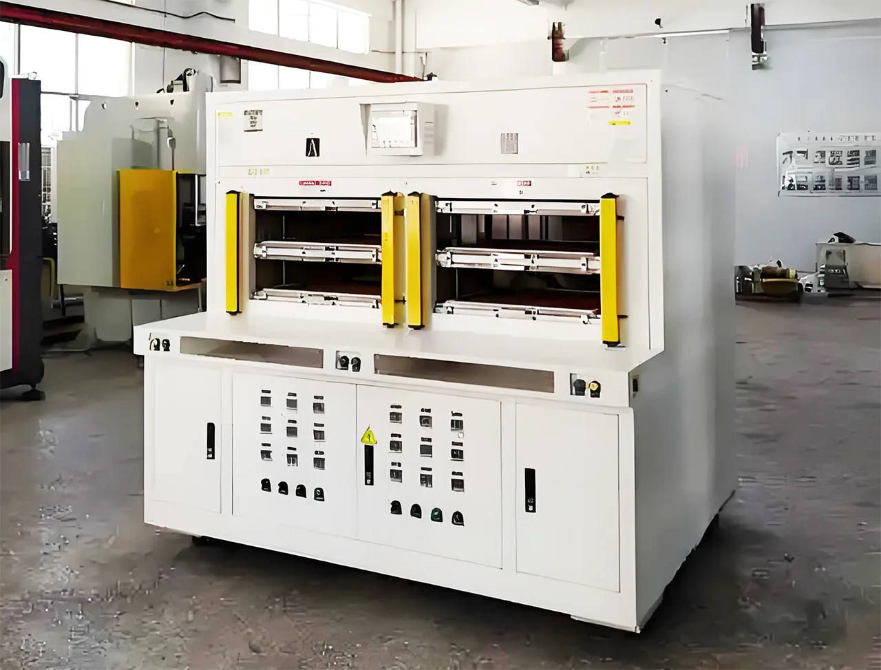
Lamination Machine
The flex pcb manufacturing process requires unique techniques compared to standard rigid boards. Below are the major steps involved:
Layer Preparation
Thin copper foil and polyimide-based films are cut to precise dimensions.
Adhesive layers are applied to ensure proper bonding.
Stack-Up Alignment
The circuit design must be aligned with high accuracy.
Optical registration systems prevent misalignment of thin, flexible sheets.
Heat and Pressure Application
The stack is subjected to carefully controlled temperature and pressure.
This activates the adhesives and bonds the copper to the base material.
Coverlay Material Application
Instead of a standard solder mask, flexible circuits use a polyimide coverlay material.
It provides insulation while allowing flexibility in bending areas.
Final Surface Finish and Electrical Testing
A surface finish (ENIG, OSP, or immersion tin) is applied for solderability.
Electrical testing ensures strong electrical conductivity and mechanical reliability.
This specialized lamination process enables flexible printed circuits to withstand repeated bending, high-density interconnections, and high temperature environments.
The Rigid-Flex Lamination Process
The rigid-flex lamination process bonds rigid FR4 areas and flexible polyimide areas in one pressing cycle. However, the two material systems behave differently under heat and pressure.
Three points decide yield:
- Selective bonding. Adhesive goes only where layers must join. Flex zones that must stay free get no bond.
- Air gap control. Gaps and unbonded zones need support, or the press crushes them. Our note on rigid-flex PCB air-gap process optimization covers the set-up.
- Thickness balance. Unequal stacks need fillers or shims. Otherwise pressure lands unevenly, as shown in Unequal-Thickness Rigid-Flex PCB Single-Press Lamination Pro.
Consequently, many shops use one press cycle with fillers instead of multi-step bonding. Rigid-flex PCB manufacturing then continues with drilling, plating and outer-layer work. For the wider picture of Rigid-Flex PCB Technology, review our process library.
Rigid, Flex and Rigid-Flex Lamination: Process and Material Comparison
| Item | Rigid PCB lamination | Flexible PCB lamination | Rigid-Flex PCB lamination |
|---|---|---|---|
| Base material | FR4 core | Polyimide film | FR4 plus polyimide film |
| Bonding layer | Glass-based prepreg | Adhesive film or prepreg | Prepreg in rigid areas; adhesive film at transitions |
| Surface protection | Solder mask | Coverlay | Solder mask plus coverlay |
| Typical press character | Higher temperature and pressure | Lower temperature and pressure | Mixed window with fillers and selective bond |
| Main risk | Warp, resin starvation | Wrinkles, peeling, dimensional shift | Air-gap crush, uneven pressure, layer shift |
| Material selection note | Match prepreg flow to copper density | Match adhesive to bend and heat needs | Balance CTE and bond selectively |
The table shows why one press recipe cannot serve all three. A profile tuned for FR4 can over-cure a thin polyimide stack. A flex-only recipe may under-cure rigid sections in a rigid-flex build. Therefore, each build needs its own window, tooling and handling plan.
Common Defects, Causes and Fixes
| Defect | Likely cause | Fix |
|---|---|---|
| Air bubbles or voids | Trapped air, weak vacuum | Improve vacuum, slow the ramp rate |
| Delamination | Poor adhesion, damp material | Dry materials, verify bond strength |
| Board warp | Uneven cooling, stress build-up | Cool under pressure, balance the stack |
| Resin starvation | Low pressure, aged prepreg | Check prepreg shelf life, adjust pressure |
| Layer misalignment | Weak registration, material shift | Tighten tooling, control film movement |
| Coverlay wrinkles | Excess heat or pressure on flex | Lower temperature, gentler press |
Inspection closes the loop. Peel strength tests check the bond line, while thermal shock, cross-sections, X-ray and AOI catch hidden shifts. Next, teams log the press curve so a good run can be repeated.
PCB Lamination Glossary
- Prepreg: Resin-impregnated glass fabric used as the bonding layer in rigid boards.
- Coverlay: Polyimide film with adhesive that protects and insulates flex traces.
- Resin flow: Movement of resin under heat and pressure; it fills gaps but can starve if too low.
- Tooling pin: Alignment pin that passes through panel tooling holes to keep layers registered.
- Release film: Sacrificial film that prevents the stack from sticking to press plates.
- Air gap: An intentionally unbonded flex zone in a rigid-flex board.
- Sub-lamination: Pressing a partial sub-stack before the final lamination cycle.
- Sequential lamination: Building a multilayer board through multiple press and drill cycles.
- Dimensional stability: How well a film or core keeps its dimensions through heat and pressure.
Applications of Flex and Rigid-Flex Lamination
Flexible and rigid-flex boards serve mobile phones, consumer electronics, medical devices, industrial automation and automotive systems. Each market sets its own bend and heat limits, so the press profile follows the use case.
Common builds include side key FPC, display FPC, sensor FPC and transfer FPC. Long or narrow parts, such as a Wire Harness-Like FPCB Manufacturing Process, depend on stable registration during lamination.
For material and stack-up questions, the PCB Manufacturing FAQ answers the most frequent ones. Also, our flex PCB assembly team can review the full flow from film to finished circuit.
FAQ
What is PCB lamination?
PCB lamination is the pressing step that bonds copper foil, prepreg or adhesive and a base material into one board. Heat and pressure cure the bond, so the layers act as a single structure with good conductivity and mechanical strength. It is used for rigid multilayer boards, flex circuits and rigid-flex boards.
Why does flexible PCB lamination use lower temperature and pressure?
Polyimide film and ultra-thin copper foil are more sensitive to heat than FR4. Higher heat can cause wrinkles or peeling in the substrate. Therefore, flexible PCB lamination runs at a lower temperature and lighter pressure, with tighter control of alignment and resin flow.
How does the rigid-flex lamination process differ from standard lamination?
A rigid-flex lamination process bonds FR4 areas and polyimide areas in the same stack. Adhesive is applied selectively, air gaps need support, and uneven thickness needs fillers or shims. Standard rigid lamination presses a uniform stack and does not face these constraints.
What causes bubbles and delamination in PCB lamination?
Bubbles usually come from trapped air or moisture, so vacuum quality and material drying matter most. Delamination points to weak adhesion, aged prepreg or a poor press profile. Both defects are easier to prevent than to repair after drilling and plating.
What is the difference between sequential lamination and sub-lamination?
Sequential lamination builds a board in multiple press and drill stages. Sub-lamination presses a smaller sub-stack before final bonding. Both are advanced methods for layer count and registration. They are not the default for most rigid, flex or rigid-flex builds; use them when the design or yield demands tighter control.
What are typical PCB lamination parameters?
Typical starting windows are 180–200°C and 200–400 psi for rigid FR4, 160–180°C and 80–200 psi for flexible polyimide, and 170–190°C and 150–300 psi for rigid-flex. Vacuum below 10 mbar and a controlled ramp of 1–5°C/min are common. Always confirm with the material datasheet, because resin chemistry and stack height shift the window.
How do I choose materials for rigid, flex and rigid-flex lamination?
Match the base material, bonding layer and surface protection to the mechanical and thermal load. Rigid boards usually use FR4 and glass-based prepreg. Flex circuits use polyimide, thin copper and adhesive film or coverlay. Rigid-flex builds need both systems plus fillers and selective bonding at transitions. Check CTE, bend requirement, moisture sensitivity and prepreg shelf life before release.
Related Posts
- PCB Etching Process: Flexible PCB & Rigid Flex Manufacturing
- PCB Surface Finish Types Explained
- Rigid-Flex PCB Air-Gap Process Optimization for High Yield — Related article
- Rigid-Flex PCB manufacturing Guide — Related article
- Unequal-Thickness Rigid-Flex PCB Single-Press Lamination Pro — Related article
- Wire Harness-Like FPCB Manufacturing Process Guide — Related article
- Flexible PCB: Features, Design Guide & Applications — Related article