Rigid-Flex PCB Air-Gap Process Optimization for High-Yield Flexible Circuit Manufacturing(Part I)

With the development of rigid-flex boards and multi-layer high-density interconnect (HDI) flexible printed circuits, manufacturers have widely adopted multi-dimensional bending in rigid-flex boards and multi-layer flexible printed circuits.
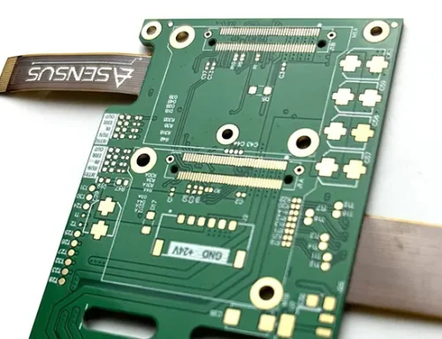
These technologies are widely used in consumer electronics such as smartphones, tablets, and wearable devices.
Flexible printed circuits offer high reliability and excellent flexibility, characterized by high wiring density, light weight, thin profile, and bendability.
To meet the bending requirements of the flexible sections, air-gap (layered) design has become a common approach in the manufacturing of such flexible printed circuits.
However, traditional designs often cause surface unevenness after completing the panel layout and lamination processes.
 Stacked Structures")
Figure 1: Introduction to the Design of Layered (Air Gap) Stacked Structures

Figure 2: Schematic diagram illustrating the mechanism behind the elevation differences created by the layered design

Figure 3: Schematic diagram illustrating the mechanism behind the height difference formed after via metallization
Rigid-flex boards with an air-gap structure undergo a process involving pure adhesive drilling, panel layout and lamination, mechanical drilling, and electroplating; as a result, the substrate surface develops areas with height differences characterized by raised and recessed sections.
At the bottom corners of the copper on the air-gap surface, the dry film may not adhere properly, appearing as bubbles.
The dry film fails to bond tightly to the copper surface, resulting in bubbles after film application, peeling after development, and open circuits or notches after etching.
The initial SET yield for the target product was only 87.4%. To address the issues caused by air gaps, this paper explores the processes and methods for manufacturing rigid-flex circuit boards with air-gap designs through testing and research.

Figure 4: Schematic diagram showing the height difference between the shelves
Experimental Section
Laboratory Instruments and Equipment
| Experimental Equipment & Instruments | Model | Manufacturer |
|---|---|---|
| Horizontal electroplating line | HKD-ALH20P | Kede |
| Mechanical drilling machine | ND-6L180E | Hitachi |
| Dry film etching machine | 08SF20NFAAA01A1 | Dongguan Yuyu Circuit Board Equipment |
| Wet film laminating machine | YTL-M630 | Duantian Chemical |
| Vacuum laminating machine | MWZK-ONE610 | Zhongshan Mingwei Automation Equipment Co., Ltd. |
| Precision semi-automatic printer | ATMA 0E56 | Dongyuan |
| Scanner and inspection machine | Ultra fusion200 | KLA |
Table 1. Experimental Instruments and Equipment
Test Materials
Resist dry film (30/40/50 μm thickness), wet film (A-9000), and two-layer (1+1 stack-up) flexible printed circuit boards.
| Material No. | Stack-up Structure | Material Type | Material Supplier | Specification |
|---|---|---|---|---|
| 40630 | 1+1 | L1 FCCL | Thinflex | 18 μm Cu / 12.5 μm PI |
| AD Adhesive | Taiflex | 25 μm AD Adhesive | ||
| L2 FCCL | Thinflex | 18 μm Cu / 12.5 μm PI |
Table 2. Two-Layer Board Stack-up Information

Table 3: Experimental Board Design Specifications
Experimental Process Flow
Main experimental process flow: Layout of two-layer boards → Drilling of through-holes → Copper plating of holes → Pretreatment → Film application → Exposure → Etching → Optical inspection.

flow chart
The study primarily focuses on layout, pretreatment, and pattern formation (including film application, exposure, and development/etching).
A Study of Different Layout Methods
Common lamination methods for flexible printed circuits include high-speed press lamination and transfer press lamination.
Transfer press lamination includes methods such as aluminum-sheet lamination, 160-layer lamination, and three-in-one lamination.
| Lamination Method | Lay-up Method | Experiment No. |
|---|---|---|
| Fast Lamination | Aluminum sheet lay-up | 1 |
| Fast Lamination | Aluminum sheet lay-up | 2 |
| Conventional Lamination | 160 lay-up | 3 |
| Conventional Lamination | Three-in-one lay-up (30 μm matte release film) | 4 |
| Conventional Lamination | Three-in-one lay-up (50 μm transparent release film) | 5 |
Table 4: Experimental Plan for Lamination Methods

Figure 5: Method for stacking aluminum sheets under high pressure

Figure 6: Method for laminating 160 layers of plates using a press

Figure 7: Three-in-one laminate pressing method using a press

Table 5: Results of graphic production using different stacking methods
Note: Figures 4, 5, and 6 show the lamination methods described in this article.
Based on the experimental results, the bubble rate and yield rate are as follows: pressure transfer + 3-in-1 lamination (50 μm transparent film) > pressure transfer + aluminum sheet lamination > pressure transfer + 3-in-1 lamination (30 μm matte film) > pressure transfer + 160 lamination > quick press + aluminum sheet lamination.
However, reliability testing of the rapid lamination + aluminum sheet stacking method revealed issues such as insufficient compression and panel rupture.
Therefore, pressure lamination combined with 160-layer stacking proved to be the optimal layout method.
However, changing the layout alone does not improve the target product’s yield rate; other methods must provide further enhancements and improvements.
A Study of Common Processes in the Pattern Transfer Process
The current main process flow for pattern transfer is: pretreatment → film application → exposure → development → etching.
This paper fixes the production of the dry film for circuit lines as a wet film application process; a wet film applicator applies the film, as shown in Figure 8.

Figure 8: Wet Film Coating Machine

Table 5: SEM Results for Different Pretreatments

Figure 9: Schematic diagrams of horizontal and vertical film application
Based on the known factors affecting the existing pattern transfer process, a DOE (Design of Experiments) analysis was conducted, as shown in Table 6.
This analysis investigated the impact of different pretreatments, dry film thicknesses, and film application methods on the yield of the target circuit pattern fabrication, thereby identifying the most effective optimal parameters and conditions for pattern transfer.
| Pretreatment Method | Dry Film Thickness (μm) | Lamination Direction |
|---|---|---|
| Chemical Cleaning | 30 | Horizontal Lamination |
| Roughening | 40 | Vertical Lamination |
| Mechanical Brushing | 50 | N/A |
Table 6: Experimental Factors and Levels
| Pretreatment Method | Dry Film Thickness (μm) | Lamination Direction | SET Yield (%) |
|---|---|---|---|
| Roughening | 30 | Horizontal | 94% |
| Roughening | 30 | Vertical | 73% |
| Chemical Cleaning | 30 | Horizontal | 86% |
| Chemical Cleaning | 30 | Vertical | 66% |
| Mechanical Brushing | 30 | Horizontal | 69% |
| Mechanical Brushing | 30 | Vertical | 59% |
| Roughening | 40 | Horizontal | 81% |
| Roughening | 40 | Vertical | 72% |
| Chemical Cleaning | 40 | Horizontal | 86% |
| Chemical Cleaning | 40 | Vertical | 94% |
| Mechanical Brushing | 40 | Horizontal | 73% |
| Mechanical Brushing | 40 | Vertical | 83% |
| Roughening | 50 | Horizontal | 72% |
| Roughening | 50 | Vertical | 52% |
| Chemical Cleaning | 50 | Horizontal | 86% |
| Chemical Cleaning | 50 | Vertical | 86% |
| Mechanical Brushing | 50 | Horizontal | 66% |
| Mechanical Brushing | 50 | Vertical | 80% |
Table 7: DOE Experimental Results
A statistical analysis of the DOE test data shown in Figure 9 reveals the following yield rates: for different dry film thicknesses, the yield rate for 40 μm > 30 μm > 50 μm; for different pretreatments, the yield rate for super-coarsening > chemical cleaning > mechanical brushing; and for different film application methods, the yield rate for vertical application > horizontal application.
A comprehensive analysis indicates that super-roughening combined with a 40 μm thick dry film (AQ-4088) and vertical application achieves the best circuit yield.
However, defects such as poor exposure and open circuits still occur in the air-gap regions, requiring the incorporation of additional improvement methods into the standard film application process.

Figure 10: Analysis of DOE Experimental Results
Study using the dry film + back pressure method
Principle of dry film lamination: A laminator presses a photosensitive dry film onto the copper surface.
The dry film is the key material for circuit formation. It consists of a three-layer structure: a polyester film, a photosensitive resist layer, and a polyethylene protective film, as shown in Figure 12.

Figure 11: Schematic of a dry film structure

Figure 12: Dry film lamination process
The key component of the dry film is the photoresist layer, while the polyester film and polyethylene protective film both serve as protective layers.
The photoresist layer exhibits excellent filling properties, allowing a dry film laminator to laminate it onto the board surface. Figure 13 shows the dry film lamination process:
 region air pocketscompaction issues")
Figure 13: Air gap (layered) region air pocketscompaction issues
When an air-gap (layered) design is used, the board surface becomes uneven.
The photoresist layer of the dry film cannot fill the height differences created by the layered design, resulting in bubbles or areas where the film does not compact properly.
Attempted Process Improvement: Secondary Pressing
Based on the phenomenon shown in Figure 13, we will attempt to apply a second pass of pressure to the board with the dry film already applied to enhance the bond between the dry film and the board surface.
We will conduct tests to determine whether this improves issues such as bubbles and poor adhesion. Table 8 below shows the test plan.
| Experimental Scheme | Specific Method | Remarks |
|---|---|---|
| Re-pressing after lamination | Re-press before exposure | / |
| Re-press after exposure | / | |
| Re-press both before and after exposure | / |
Table 8: Dry Film Re-Pressing Plan

Table 9: Dry Film Back Pressure Test Results
The experimental results show that after applying the dry film to the board surface with an air-gap (layered) design, re-pressing the board with the hot roller of the laminator did not improve the presence of bubbles or poor adhesion on the board surface; instead, it resulted in a large number of exposure defects and over-etching.
Applying dry film followed by re-pressing cannot resolve pitting and surface unevenness caused by the air-gap (layered) design; therefore, other process solutions need testing.
Continue reading: Part 2 «