
PCB Copper Plating Process for Reliable Conduction
Introduction
Copper plating is the step that turns drilled holes into conductive paths. A controlled copper layer is deposited on hole walls and trace surfaces, so every plated through hole carries current and every trace stays intact after bending. In [flexible circuits](https://gekunflex.com/flexible-circuit/), flex PCB copper plating carries an extra burden: it has to hold up under repeated flexing and thermal cycling, not merely pass a continuity check once. Getting there starts before the plating tank. Black hole pre-treatment FPC lines replace or supplement electroless copper with a carbon-based conductive layer that anchors the deposit, which matters most on microvias and awkward via shapes. What follows walks the process in order — drilling and cleaning, pre-treatment, electroplating, pattern imaging, inspection — then covers the parameters that govern thickness and throw power, the defects that appear on the line and how to correct them, and the acceptance tests that confirm reliable conduction.
In the fabrication flow, plating sits between lamination and outer-layer imaging: inner layers are imaged and etched, the stack is laminated, holes are drilled, and the walls are metallized and built up to final thickness before the outer pattern is defined. Every step downstream inherits whatever the plating line produced, which is why the settings discussed later are treated as process controls rather than production targets.
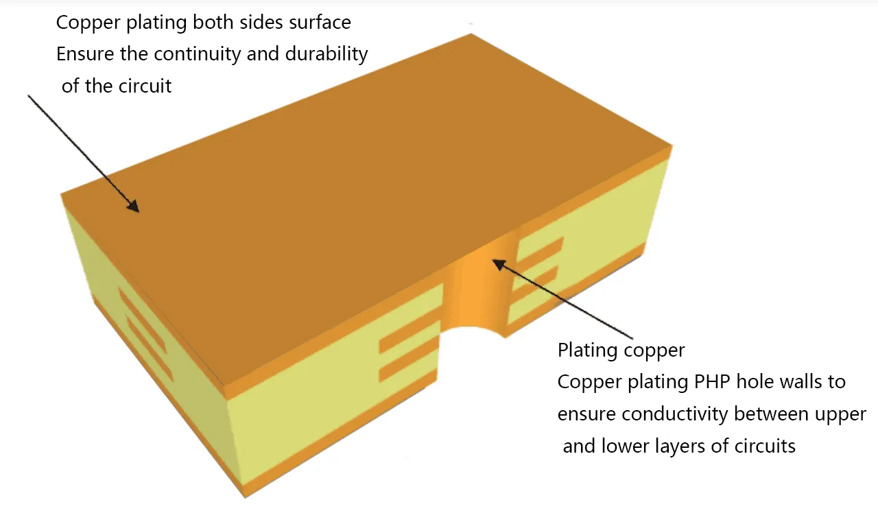
The Role of Copper Plating in Flexible PCBs
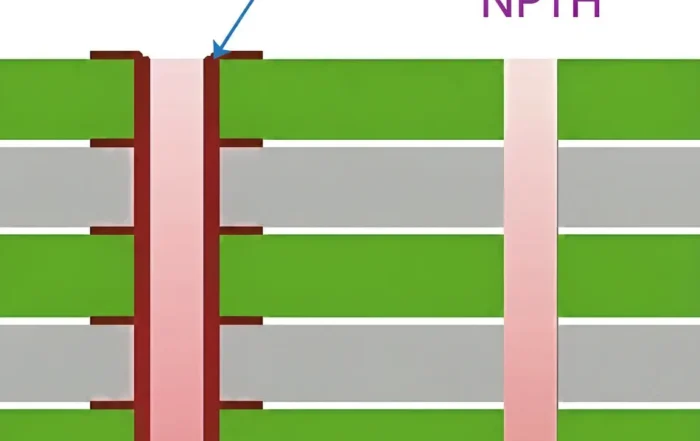
Copper plating provides a continuous electrical path across layers of flexible circuits. Its functions include:
- Strengthening copper traces for bending and flexing.
- Ensuring reliable conductivity in plated through holes.
- The design combines flexible and rigid layers to support rigid flex plating.
- Enabling high-density layouts without signal loss.
Furthermore, copper plating also influences the long-term reliability of the board. Poor plating may result in the form of open circuits, signal loss, or mechanical failure. Engineers use professional electroplated copper or rolled annealed copper for applications that require repeated bending and harsh conditions.
Reference: DuPont Flexible Circuit Materials
Pre-Treatment and Black Hole Process
Before any copper goes down, the hole wall has to accept it. Electroless copper is the traditional route: a chemical reduction lays a thin seed layer over the dielectric, and electroplating builds on that seed. The Black Hole process takes a different path — panels pass through a carbon dispersion, and the conductive layer is held by a combination of physical adsorption and chemical bonding rather than by a chemical reduction step. On polyimide and other flex dielectrics this tends to give a more uniform seed on microvias and non-circular vias, reduces void formation in deep holes, and removes the wastewater burden that electroless copper lines carry. Neither route is universally better; the choice follows via geometry, dielectric, and the defect history of the line.
Either route still serves the same goal: strong plated-through holes and surface copper traces in the flex PCB copper plating process.
Step-by-Step Copper Plating Process
The sequence below runs from bare laminate to a verified plated panel. Each step sets up the next, and skipping ahead — plating before the hole wall is properly prepared, for instance — resurfaces later as voids or thin walls that no amount of final inspection can recover.

Step 1 – Drilling and Cleaning
Holes are drilled in the substrate material (typically polyimide films) and cleaned thoroughly. The PCB cleaning process removes debris, resin smears, and contaminants. Proper material preparation ensures uniform plating and strong adhesion in subsequent steps.
Step 2 – Pre-Treatment
Pre-treatment may include electroless copper or the Black Hole process for enhanced adhesion. This step is critical to ensure all plated through holes are conductive and ready for copper deposition.
Step 3 – Electroplating Process
The electroplating process deposits copper onto the prepared surfaces. Engineers control copper thickness to meet both electrical and mechanical requirements. For flex circuits, rolled annealed copper is best for bending areas because it is flexible. On the other hand, electro-deposited copper works well in rigid areas with fine circuit patterns.
Step 4 – Photo-Imaged Circuit Pattern
A photo-imaged resist defines the circuit pattern on surfaces, ensuring only designated areas receive copper plating. This step is critical for achieving high-density layouts without short circuits.
Step 5 – Inspection and Quality Control
Inspection verifies:
Continuity of all plated through holes.
Correct copper thickness across the board.
Absence of voids or peeling.
Quality control ensures that rigid flex PCBs and flexible circuits perform reliably in demanding applications.
Design and Manufacturing Considerations
Careful design and manufacturing practices enable more effective flexible PCB copper plating.
- Stack: Layered structures have to be platable without delaminating.
- Copper thickness: If the copper plating is too thick, it can be hard to bend. If it is not thick enough, it can affect conductivity.
- Circuit pattern: Fine-pitched designs can afford the finest control of plating to avoid shorts.
- Plating process parameters: Optimize current density, temperature, and agitation for best results.
- Adhesion improvement: The Optional Black Hole process can enhance reliability in microvias.
Manufacturers often do small tests on flexible printed circuit boards. They do this to improve the electroplating process before starting full production.
Reference: IPC-6013 Flexible/Rigid-Flexible Printed Boards Standard
Vertical Plating vs VCP: Uniformity, Throw Power and Capacity
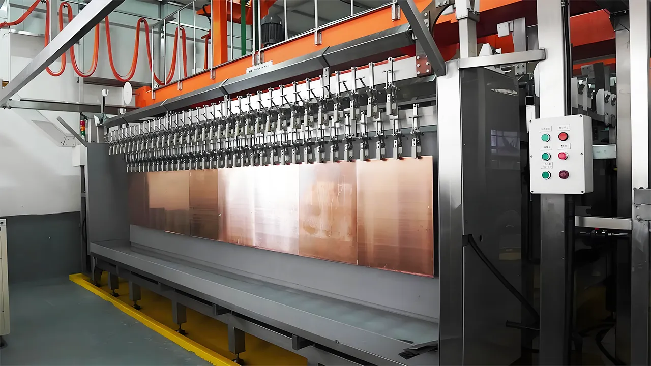
Traditional vertical plating uses racks and batch tanks. Panels move through static or agitated baths, and current distribution depends on rack contact, shielding and bath flow. VCP (vertical continuous plating) moves panels through a continuous line with controlled flow and current zones. The comparison below focuses on the production outcomes that affect reliable conduction.
| Factor | Traditional vertical plating | VCP |
|---|---|---|
| Thickness uniformity | Good with tight rack control, but edge and contact effects can widen spread | Generally tighter within-panel and panel-to-panel spread because flow and current are controlled continuously |
| Throwing power / deep-hole coverage | Depends strongly on agitation and chemistry; high aspect ratio holes need extra care | Better flow at the hole mouth and through the hole supports throw, but chemistry and current profile still set the limit |
| Capacity | Batch-based; throughput scales with tank size and racks | Continuous flow supports higher throughput and shorter queue time |
| Best fit | Flexible volume mixes and older lines with strong process control | High-mix HDI and multilayer boards that need consistent via walls at volume |
VCP is not automatically better for every product. It earns its place when uniformity and capacity matter together. For high-aspect-ratio through holes, both approaches still need correct current density, bath maintenance, and agitation. The decision should be based on the product’s via geometry, copper thickness target, and volume—not on equipment fashion.
Key Parameters That Control Thickness and Throw
Uniform copper comes from several linked settings. Current density sets the deposition rate and the crystal structure. Agitation and filtration keep fresh chemistry at the hole wall, which improves throw power in deep holes. Bath chemistry, temperature, and plating time decide the final copper thickness. So a stable recipe is a reliability tool, not just a production number.
Aspect ratio is the board thickness divided by the hole diameter. As aspect ratio rises, fresh electrolyte reaches the hole center less easily, so throwing power (TP) becomes the limiting metric. TP is usually expressed as the ratio of copper thickness at the hole center to thickness at the surface. A higher TP means more uniform wall coverage and a lower risk of a thin, hot spot in service.
Through-hole plating and blind-via filling are different targets. Through holes need a continuous, uniform wall. Blind vias may need bottom-up fill for stacked or staggered HDI designs. Fill additives, current profiles, and circulation must be balanced; over-filling can create bumps, while under-filling leaves voids. Thermal stress and thermal cycling tests then confirm whether the copper-to-wall interface survives expansion and contraction.
Also, bath maintenance protects yield. Contamination, anode wear, and weak filtration all raise defect risk. Therefore, most lines track chemistry daily and change filters on schedule.
Common Defects and Practical Fixes
| Defect | Typical cause | Practical fix |
|---|---|---|
| No copper in hole / missing wall metallization | Incomplete seed or activation, poor wetting, current shadow in deep holes | Verify pre-treatment coverage, improve wetting and agitation, adjust current ramp and shielding |
| Void in via wall | Trapped air, weak agitation, poor wetting | Improve agitation and wetting, verify pre-treatment coverage |
| Thin copper / low thickness | Low current density, weak throw, short time | Adjust current density, strengthen bath circulation, confirm plating time |
| Nodule at board edge | High current at edges, resist damage | Rework shielding, control the current ramp |
| Incomplete blind-via fill | Additive imbalance, low current, poor circulation | Adjust fill additives and current profile, improve flow at via bottom |
| Poor adhesion | Contaminated surface, weak seed layer | Tighten cleaning, review black hole or electroless step |
| Uneven thickness | Weak filtration, poor bath balance | Improve filtration and bath control |
Some failures come from the metal stack itself. A nickel–copper adhesion failure, for example, usually traces back to surface preparation and rinse quality. Also, base material choice matters; see FCCL vs. rigid copper clad laminate for the key differences.
Quality Checks for Reliable Conduction
Verification should answer one question: is the via wall fully covered and thick enough for the current load? A cross-section under a microscope shows wall thickness and voids. Backlight testing reveals thin or missing coverage in a fast, visual way. In addition, XRF gauges copper thickness on coupons and panels. Throwing power can be calculated from center-to-surface thickness on a coupon.
Adhesion and thermal stress tests close the loop. Thermal shock or cycling exposes weak interfaces before delivery; record resistance change and inspect for wall cracks. For high-aspect-ratio or blind-via builds, add fill-void inspection and focused cross-sections at the worst-case via. Insulation also needs attention on thick copper builds; FPC Insulation Performance covers that side. For production questions, the PCB Manufacturing FAQ collects common answers.
Safety, Environmental Controls and Wastewater Treatment
Copper plating uses acidic baths, copper salts, and organic additives, so the line needs more than a recipe. Fume extraction, PPE, and secondary containment protect operators. Rinse water is segregated and treated; common steps include pH adjustment, precipitation, ion exchange or electrowinning, and discharge monitoring. Bath life extension and drag-out reduction cut both waste and chemical cost. These controls do not change the plating physics, but they are part of a stable, repeatable process.
Scope and Applicable Boundaries
This page focuses on copper plating for rigid and flex multilayer through holes and HDI blind/microvias. It does not cover surface finish selection (ENIG, OSP, immersion tin) or RF material choice, which are separate decisions. Use the process guidance here to set thickness, coverage, throw power, and verification targets, then confirm the final stack with the fabricator.
Applications and Advantages of Flex PCB Copper Plating
Well-controlled plating supports several product families. Consumer electronics, medical devices, automotive modules, and industrial automation all use flexible circuits with plated vias. High-density designs benefit most, because microvias need full wall coverage.
In addition, plating enables rigid-flex designs that combine flexible and rigid layers. Teams planning such a build can review Rigid-Flex PCB Technology before layout. Also, the Rigid-Flex PCB product line shows how plating fits the stack. For demanding programs, High-Reliability Flexible Circuits for High-End Applications explains the extra controls used.
The advantages stay consistent: stable conduction, longer flex life, and fewer field failures.
Key Takeaways
Reliable conduction is not created by a single plating step. It is the result of a complete chain: a continuous seed layer, enough copper thickness on the wall, sufficient throwing power for the aspect ratio, controlled blind-via filling where needed, and verification by cross-section, backlight, XRF, and thermal stress. VCP can tighten uniformity and capacity, but it only helps when bath chemistry, current profile, and agitation are in control. When the chain is intact, plated through holes carry current with lower resistance, survive thermal cycling, and keep flexible circuits working through repeated bending.
FAQ
What does black hole pre-treatment do in FPC plating?
Black hole pre-treatment forms a carbon-based conductive layer on via walls. It combines physical adsorption with chemical bonding. This helps plating adhere and reduces defects, especially on microvias and unusual via shapes.
How thick should plated copper be?
Thickness follows the design. Current load, bend radius, and mechanical stress set the target. Engineers then control current density, bath chemistry, temperature, and time to reach it. Thicker copper helps current and flex life, but it also raises etch and insulation demands.
What is blind via filling and when is it needed?
Blind via filling deposits copper into a via that does not go through the whole board, often for stacked or staggered HDI. It is needed when the design requires a flat, conductive surface over the via or when reliability depends on a void-free copper plug. Fill additives, current profile, and circulation must be balanced; under-fill leaves voids and over-fill creates bumps.
What is throwing power (TP) and why does it matter?
Throwing power describes how well copper plates deep into a hole compared with the surface. It is commonly measured as the ratio of center-wall thickness to surface thickness. High aspect ratio holes are harder to plate, so TP becomes the limiting factor for uniform wall coverage, current capacity, and thermal reliability.
How can I verify wall integrity?
Use a mix of methods. A cross-section shows wall thickness and voids. Backlight testing exposes thin coverage quickly. XRF checks surface thickness. Add thermal shock or cycling to prove adhesion before the board ships; record resistance change and inspect for cracks.
Related Posts
- Carbon-Coated Film Evaluation for Reliable FCCL Copper Plating — Related article
- Nickel–copper adhesion failure in flexible PCBs | Causes & Fixes | Gekun — Related article
- Enhancing FPC Insulation Performance — Related article
- FCCL vs. Rigid Copper Clad Laminate: Key Differences — Related article
- FPCB Differential Impedance Optimization with Mesh Copper — Related article