
Optimization of Differential Impedance in FPCB Using Mesh Copper Reference Layer
However, differential impedance is the impedance a differential pair sees when its two traces carry equal and opposite signals. Therefore, on an FPCB, a mesh copper reference layer changes that value because the mesh is not a solid plane. Additionally, this guide explains how mesh geometry shifts differential impedance and how to keep it on target.
Meanwhile, see also High-Reliability Flexible Circuits for High-End Applications for related specifications.
For example, see also Rigid-Flex PCB Technology for related specifications.
What Differential Impedance Means in an FPCB
In addition, differential impedance is the impedance seen by the difference signal on a pair of coupled traces. As a result, each trace carries half the signal, with opposite polarity. In practice, without coupling, the value depends mainly on the capacitance per unit length of a single line. Next, with tight coupling, both capacitive and inductive coupling shape the result.
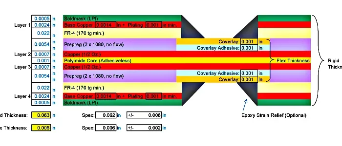
Therefore, pair geometry and the reference plane set the target. Consequently, in a Flexible PCB, three more variables enter. Moreover, they are the polyimide dielectric constant, the adhesive thickness, and the coverlay. In particular, for a broader view of this topic, see High Frequency Flexible PCB Impedance Control.
Why Mesh Copper Reference Changes FPCB Differential Impedance Control
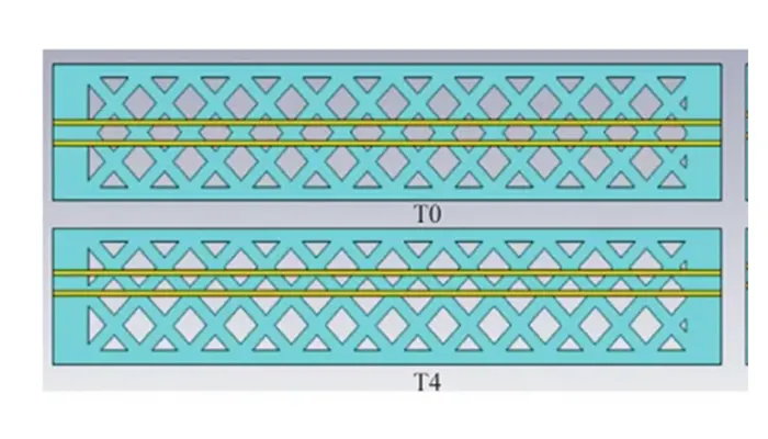
However, a solid plane gives a continuous return path. A mesh plane does not. It is a grid of copper lines with open windows, so part of the field passes through those windows and the effective reference moves farther away.
Two effects follow. First, the effective dielectric height rises, which usually pushes differential impedance up. Second, return current must flow around the openings. That adds local inductance and creates impedance ripple along the pair.
Mesh copper still earns its place. It keeps flexibility, saves weight, and reduces copper stress in bend areas. The trade-off is that FPCB differential impedance control becomes geometry-dependent. Treat the mesh as a design variable, not as a background layer.
Key Mesh Parameters That Shift Differential Impedance
Open ratio
Open ratio is the copper-free area inside a mesh window. A higher open ratio means a weaker reference. As a result, impedance rises and ripple grows.
Mesh line width and pitch
Wider mesh lines and tighter pitch make the grid behave more like a solid plane. In practice, designers often compare open ratios in the 30–50% band. Then they pick the densest grid that still meets bend requirements.
Orientation
Mesh lines running parallel to the pair create long continuous return paths. A 45° or perpendicular orientation spreads return current more evenly.
Equivalent modeling
Field solvers need an equivalent plane model. Replace the mesh with a plane at an effective height, and adjust the effective dielectric constant. In addition, confirm the model on a test coupon before release.
Worked Parameter Table: Line Width, Gap, and Dielectric Thickness to Differential Impedance
Use this table as a starting window, not a release tolerance. The values assume a polyimide FPCB with Dk 3.3–3.5, 1 oz copper, a mesh open ratio of 35–45%, and an equivalent mesh reference height of about 1.10–1.25 times the nominal dielectric thickness. The mesh window is continuous under the pair.
| Target differential impedance | Trace width W (mm) | Gap S (mm) | Nominal dielectric thickness H (mm) | Equivalent mesh height H_eff (mm) | Expected differential impedance range (Ω) |
|---|---|---|---|---|---|
| 85 Ω | 0.18–0.22 | 0.10–0.14 | 0.10 | 0.11–0.125 | 84–95 |
| 90 Ω | 0.16–0.20 | 0.10–0.15 | 0.10 | 0.11–0.125 | 88–99 |
| 100 Ω | 0.13–0.17 | 0.13–0.18 | 0.10 | 0.11–0.125 | 96–110 |
Worked example: start with a 90 Ω target, W = 0.18 mm, S = 0.13 mm, H = 0.10 mm, and Dk = 3.4. A solid-plane model lands near 88 Ω. At a 40% open ratio, the equivalent mesh height rises to about 0.12 mm, and the same geometry models at roughly 94–98 Ω. To return toward 90 Ω, reduce S to about 0.10 mm or increase W to about 0.20 mm, then confirm the result on a TDR coupon. For 100 Ω, the table shows a narrower line and wider gap; if the mesh pushes the result above the window, increase coupling before you increase stack height.
Design Rules for Mesh Copper Reference FPCB
- Keep each pair over one continuous mesh window. Do not let the pair cross a window boundary.
- Never route a pair across a mesh gap that runs parallel to the pair.
- Add cross-tie copper or stitching vias beside the pair when the reference switches layers.
- Place the mesh at 45° to the pair in bend regions with high stress.
- Avoid narrow mesh necks under connectors, where current density is highest.
- Keep the pair symmetric. Skew, not just impedance, decides whether the link closes.
For build-related questions, our PCB Manufacturing FAQ covers stackup, material, and tolerance topics.
Workflow: From Target Impedance to Verified Result
1. Set the target. Common values are 85 Ω, 90 Ω, or 100 Ω differential, depending on the interface.
2. Run a first calculation with trace width, gap, dielectric thickness, Dk, and copper thickness.
3. Model the mesh at the chosen open ratio, using an equivalent reference height.
4. Build a coupon and measure it with TDR against the target window.
5. Iterate once, then freeze the stackup for production.
Verification matters more here than on a solid plane. Use the PCB testing methods in our test guide for continuity, isolation and time-domain checks. Also record coupon data per lot, because mesh etching tolerance shifts with copper thickness. Gekun, a flex PCB manufacturer in Shenzhen since 2014, builds those coupons on the production stackup.
Solid Copper vs Mesh Copper Reference: Quick Comparison
| Item | Solid copper plane | Mesh copper reference |
|---|---|---|
| Impedance consistency | High, predictable | Medium, depends on open ratio |
| Return path | Continuous | Fragmented at windows |
| Bending reliability | Lower, higher stress | Better, lower stress |
| Weight and copper use | Higher | Lower |
| Modeling effort | Standard formulas apply | Needs an equivalent plane model |
The table shows the trade-off clearly. A mesh reference is a mechanical choice that carries an electrical cost. Therefore, define the electrical budget first, then choose the mesh.
Common Mistakes in FPCB Differential Impedance Control
The most common error is copying a rigid board result onto a mesh. A rigid stackup assumes a solid plane, so the calculated value comes out too low. Another mistake is ignoring the coverlay, which adds capacitance and lowers impedance.
A third error is a reference switch without stitching vias. Current must jump between layers, and the return path breaks. Rigid-Flex PCB layouts hit this most often, because the reference changes between flex and rigid sections.
Finally, some teams verify only one coupon. Mesh etching varies across a panel, so sample more than one location on high-volume flexible circuit boards.
FAQ
Can mesh copper be used as a differential reference plane?
Yes, when the pair stays over one continuous window, and the mesh is dense enough. Mesh copper reference FPCB designs work well for bending and weight-critical products. However, the pair must be re-simulated with an equivalent reference height, and the result must be confirmed by TDR on a coupon.
What open ratio is suitable for mesh copper in an FPCB?
There is no single number. Start from the densest grid the bend radius allows, then relax it only while impedance stays inside the tolerance window. Many designs settle in the 30–50% open-ratio band, but the correct value depends on dielectric height, Dk, and the target impedance.
How is differential impedance verified after fabrication?
Verification uses a TDR coupon with the same stackup, mesh pattern, and pair geometry as the product. The measured differential impedance should sit inside the agreed tolerance across the coupon length. Coupling length, intra-pair skew, and reference continuity are also checked, then compared with the field-solver model.
Related Posts
- High Frequency Flexible PCB Impedance Control Guide — Related article
- Flexible PCB: Features, Design Guide & Applications — Related article
- PCB Testing Methods: 8 Techniques for Quality Assurance — Related article
- AI-Driven Optimization of Flexible Circuit Boards Production — Related article
- Adhesive-Free FCCL Substrates vs Adhesive-Based FCCL — Related article