HDI Rigid-Flex PCB Manufacturing Process and Technical Challenges in Advanced Medical Electronics
Health is a timeless pursuit for humanity, and the demand for medical resources continues to grow. Today, the early detection and prevention of diseases have become a major focus of public attention. The emergence of portable smart medical devices for home use has, to some extent, alleviated the problem of “difficulty in accessing medical care.”
People can now receive medical care at home, enabling early detection, monitoring, and relief.
They can complete basic testing, health maintenance, and treatment without leaving their homes, eliminating the need to visit a hospital for minor ailments and reducing medical costs.
As a result, these devices have gained widespread popularity. In particular, since the onset of the COVID-19 pandemic, demand for portable home medical electronic devices—including infrared thermometers, blood glucose monitors, blood pressure monitors, pulse oximeters, digital scales, infrared therapy devices, magnetic therapy devices, home ventilators, and nebulizers—has continued to rise, directly driving a new wave of growth in the medical electronics industry.
According to statistics from the *China Medical Device Blue Book (2023 Edition)*, the portable medical electronics industry has significant growth potential and is expected to maintain a high growth rate over the next 10 years, with a promising market outlook.
The main features of portable home medical electronic devices are their compact size, portability, intuitive and simple operation.
The printed circuit boards (PCBs) used in these devices are primarily rigid-flex PCBs (R-FPCBs) and high-density interconnect (HDI) boards.
It is foreseeable that the rise and prosperity of the market for portable home medical electronic devices will inevitably bring new development opportunities to the PCB market.
This article takes a 10-layer, third-order HDI R-FPCB used in portable home medical electronic devices as an example to provide a detailed explanation of the manufacturing processes and technical challenges associated with such products.
Test Section
Product Structural Features
The key specifications of this portable medical electronic R-FPCB product are shown in Table 1, and its laminated structure is illustrated in Figure 1.
| No. | Characteristic | Technical Features |
|---|---|---|
| 1 | Product Type | 10-layer (4B+2F+4B) rigid-flex combination, 10-layer stacked blind-via HDI |
| 2 | Board Thickness | Rigid board thickness: (0.88 ± 0.089) mm, Flexible board thickness: (0.15 ± 0.05) mm |
| 3 | Laser Blind Via Diameter / mm | 0.10 |
| 4 | Minimum Mechanical Drill Hole Diameter / mm | 0.15 |
| 5 | Minimum Line Width / Spacing / mm | 0.076, 0.076 |
| 6 | Minimum Distance from Inner-Layer Metalized Hole to Trace / mm | 0.13 |
| 7 | Minimum BGA/IC Pad Size / mm | 0.15 / 0.15 |
| 8 | Trace Width Tolerance | Ordinary trace width ±20%, impedance trace width ±10% |
| 9 | Copper Thickness | Surface 235 μm, PTH 225 μm |
| 10 | Application Field | Medical Electronics |
Table 1. Key Specifications of PCBs for Portable Medical Electronics

Figure 1 Schematic diagram of the product’s laminated structure
Manufacturing Process Flow
The manufacturing methods for R-FPCBs are constantly evolving in response to technological advancements and changes in product specifications, with window fabrication (opening) technology being the most critical aspect.
Currently, the primary window fabrication techniques include through-hole fabrication, copper foil etching, mechanical depth control, and laser cutting, among others.
Different methods are suitable for products with varying structural characteristics. This product is a 10-layer, third-order HDI R-FPCB, and the design process flow is as follows.
L5/L6 (Flex Board):
Cutting → Drilling → Electroless Copper Plating → Board Plating → Via Pattern Plating → Via Plating → Stripping → Circuit Pattern Plating → Etching → Automated Optical Inspection (AOI) → Flexible board browning → Cover film windowing → Cover film application → Rapid lamination 1 → Flexible board rivet hole punching → Micro-etching → Protective tape application → Rapid lamination 2 → Board drying → Flexible board browning.
L4–L7:
Lamination [L5/L6 + prepreg (PP) + copper foil] → Drilling → Electroless copper plating → Board electroplating → Circuit pattern formation → Etching → AOI → Browning.
L3–L8:
Laminate (L4/L7 + PP + copper foil) → Pre-brown treatment for laser direct drilling (LDD) → Laser drilling → De-brown → Electroless copper plating → Full-board via filling → Circuit patterning → Etching → AOI → Browning.
L2–L9:
Lamination (L3/L8 + PP + copper foil) → LDD browning → Laser drilling → Browning removal → Electroless copper plating → Full-board via filling → Circuit patterning → Etching → AOI → Browning.
L1–L10:
Laminating (L2/L9 + PP + copper foil) → Pilot hole drilling → LDD browning → Laser drilling → Drilling → Browning removal → Electroless copper plating → Full-board via filling → Full-board plating (Negative) → Circuit patterning → Vacuum etching → Post-etch impedance testing → HTC testing → AOI → Via filling before solder mask application → Solder mask printing → Character printing → Impedance testing → Secondary drilling → Contour milling → Laser cutting → Protective tape removal → Film removal → Laser cutting 2 → Electroless nickel/ Gold → Pre-forming test → Forming → Board curvature inspection → Laser cutting 3 → Forming 2 → Shipping inspection (Final Quality Control, FQC) → Factory Quality Assurance (FQA) → Packaging.
Results and Discussion
Lid Removal and Window Opening
1. Description of Challenges
Lid removal and window opening are among the core processes in the manufacture of R-FPCBs.
Different lid removal methods have distinct characteristics and scopes of application.
In the subsequent production process, the through-window method causes significant damage to the flexible circuit board area due to chemical solutions and mechanical forces, which can easily affect product quality and appearance;
The copper foil etching method is suitable for 2–4-layer R-FPCBs but does not apply to this product.
This product consists of a sequential lamination of one flexible core layer and four copper foil layers. It lacks a rigid core layer, and the PP and copper foil layers are too thin to allow for depth-controlled milling of blind vias, making the mechanical depth-controlled method unsuitable for cover removal.
Precise adjustment of laser energy according to window thickness ensures that the rigid layer adjacent to the flexible board is fully cut through without damaging the flexible layer.
Designers typically include a dummy copper pad on the adjacent rigid layer. After windowing is completed, an etching process removes the dummy copper pad.
In this product, the windowing area contains circuit patterns and via rings that cannot undergo etching, so direct application of the conventional laser cutting method becomes infeasible.
In addition, the flexible layer is laminated to the copper foil. To prevent corrosion of circuits and disk-shaped hole rings in the flexible area—caused by copper foil wear during pretreatment or etching solution ingress during circuit etching—the process does not allow windowing of the PP layer.
However, leaving the PP layer un-windowed also poses a technical challenge, as it must prevent resin flow and powder shedding onto the flexible layer, which would compromise quality and appearance.
2. Technical Challenges
To address the technical challenges posed by the absence of a rigid core panel and the thin wall thickness at the window openings—which precluded the use of mechanical depth control and laser cutting for lid removal—this project innovated the laser cutting process for lid removal. Before lamination, a layer of protective tape is applied to the cover film of the flexible layer.
The PP layer is left uncut; instead, laser cutting is used to penetrate the PP adjacent to the flexible layer. The laser-cut gap in the PP is 0.025 mm.
During the lamination process, the overflow of low-flow PP adhesive fills this gap, preventing the ingress of chemical solutions into the flexible layer and avoiding corrosion of the circuits and via rings during subsequent processes.
Layer-by-Layer Fabrication Process
Manufacturers first complete lamination with copper foil, drilling, electroplating, board plating, and etching to finish fabrication of layers L4–L7. They etch away the copper foil at the window locations. Next, production proceeds to fabricate layers L3–L8.
Engineers use high-flow PP to fill the holes, completing resin-filled holes for layers L4–L7. They also etch away the copper foil corresponding to the window openings on layers L3 and L8.
Production then continues sequentially with layers L2–L9 and L1–L10, with operators etching away the copper foil at the window openings on each layer.
Finally, technicians perform laser cutting to align the pre-cut PP slits adjacent to the flexible layer and remove the rigid layer at the window openings, exposing the flexible layer.
Operators then remove the protective tape, completing the R-FPCB shown in Figure 2.
Using this method, applying a layer of protective tape to the cover film of the flexible layer before lamination prevents PP adhesive overflow and powder shedding into the flexible area—which would otherwise occur without windowing—thereby avoiding quality and appearance issues;
Pre-Cut PP and Lamination Behavior
The PP layers adjacent to the flexible layer are pre-cut through with a laser before lamination.
During the lamination process, the low-flow PP adhesive can fill the pre-cut laser gaps, avoiding the issues associated with conventional PP windowing processes—such as the ingress of chemical solutions into the flexible layer during subsequent processes, leading to circuit and via etching problems.
The process prevents lamination wrinkles and unevenness that could affect surface laser drilling and circuit fabrication. During circuit etching, operators remove the copper foil in the layers corresponding to the window locations, leaving only the PP layer.
A low-energy laser then burns through to the PP pre-cut seam to complete cover removal, significantly reducing the difficulty of laser cutting.
The process eliminates the need for a dummy copper pad as a buffer, and manufacturers successfully fabricate the R-FPCB.

Figure 2 Schematic diagram of the product with the lid removed and window opened
Advanced Blind and Plated-Through Hole Alignment
1. Description of Challenges
As PCBs become increasingly high-density, the alignment of patterns, blind holes, and through-holes across different layers has become a highly complex technical challenge.
In HDI rigid-flex PCB, blind vias and patterns are first fabricated on the core layers, followed by lamination layer by layer to the outer layers. Patterns and signals across layers are connected via blind vias, with only a small number of through-holes used for signal connections or as tooling holes on the outer layers.
The manufacturing process is complex, and coupled with the small size of blind and through-hole pads, the requirements for interlayer blind via alignment and overall alignment are even higher, making alignment control significantly more challenging.
The layer-by-layer alignment process for HDI rigid-flex PCB involves aligning the patterns and blind vias of the next layer based on the reference marks of the previous layer to create the blind vias and patterns for that layer.
While this process effectively controls the alignment of patterns and blind vias between adjacent layers, it has limitations when applied to high-order stacked via designs or products that incorporate both blind and through-holes.
After multiple rounds of laser drilling, electroplating, and pattern formation, alignment deviations accumulate between stacked layers.
By the time the process reaches the outermost layer, the cumulative deviation becomes significant, adversely affecting the alignment accuracy of blind vias and outer-layer through-holes, ultimately leading to quality issues such as blind hole bottom collapse and through-hole failure.
2. Technical Challenges
A new method for blind via alignment addresses the shortcomings of conventional processes.
This method places all laser drilling alignment targets on each layer and positions the outer-layer mechanical drilling alignment targets on the first laser blind via layer.
For this product, layers L3 and L8 serve this function, while any interconnecting HDI rigid-flex PCB can assign these targets to the core board layer.
The laser drilling targets for each layer and the outer layer mechanical drilling targets all reference layer L3 (with layer L8 serving as the reference on the reverse side) . Alignment for each layer is referenced to the same level, reducing misalignment caused by the cumulative effects of factors across different layers.
This improves alignment accuracy between higher-order stacked blind via layers and through-hole alignment, thereby enhancing the alignment capability of HDI products.
The specific alignment design is shown in Figure 3. In Figure 3, BU (build-up) refers to the laminate, and OL (outer layer) refers to the outer layer.

Figure 3 Alignment Design for Blind Hole Targets
(1) The L3 and L8 layers use pre-defined expansion and contraction coefficients.
Through-holes are drilled at the four corners to serve as alignment targets; both the top and bottom surfaces use these targets for alignment via laser blind holes and pattern registration.
(2) Laser Alignment Target Design for Blind Hole Lamination
Engineers also design alignment targets for lamination and outer-layer laser blind holes on Layers L3 and L8. Windows are cut at the target locations corresponding to the lamination positions to improve light transmission.
During production, a laser drilling machine applies IR light to locate these areas, then removes the copper layer through burning and scraping. The system captures the exposed target and uses it for blind hole alignment during lamination.
(3) Optimized Alignment Process for High-Order HDI rigid-flex PCB
Designers place the outer-layer mechanical drilling targets on Layer L3. X-ray drilling targets punch them out, and operators cut windows at the corresponding positions of each target layer.
The mechanical drilling machine then picks up the targets punched by the X-ray drilling machine to perform the drilling.
Designing both the multilayer and outer layer alignment targets on the same layer avoids significant misalignment issues in interlayer hole alignment caused by multiple drilling operations and pattern fabrication.
This significantly improves the alignment accuracy of multilayer stacked holes in high-order, arbitrary-layer interconnect (HDI) boards and enhances the product’s alignment capability.
Figure 4 presents a schematic comparison of conventional layer-by-layer alignment processes and the alignment process adopted in this project. Figure 5 presents a cross-section of the stacked and blind vias.

Fig 4 Comparison of Alignment Processes for Different Targets

Fig 5 Effect of designing all alignment targets on the same layer
Electroplating Filling of Blind Holes
1. Description of Challenges
One of the core processes in HDI rigid-flex PCB manufacturing is the electroplating filling of laser-drilled blind holes.
Most electroplating filling processes currently rely on full-board filling technology.
In this method, laser-drilled blind holes first undergo electroless copper plating, and a specialized filling solution then fills and levels the holes.
Additive-Controlled Electroplating Mechanism
The filling of laser-drilled blind vias relies on the principle of additive-controlled electroplating. The plating solution contains multiple additives, including brighteners, leveling agents, and carrier agents.
Brighteners show specific properties at the electrode interface. Brighteners also undergo electrostatic adsorption at the electrode interface. These behaviors influence the metal electroplating process.
The process changes the morphology and properties of the deposited layer. These changes help achieve the desired coating performance.
The carrier helps the brightener distribute throughout the recesses of the cathode. Chloride ions also support the effective function of the carrier.
As a result, the originally uneven copper plating distribution becomes more uniform. This process provides a certain degree of plating uniformity.
Role of Leveling Agents
In the acid solution, the leveling agent carries a strong positive charge. Areas with a stronger negative charge on the workpiece surface attract the leveling agent.
Such areas include protrusions, board corners, and high-current regions at hole openings. Within these regions, the leveling agent competes with positively charged copper ions.
This prevents copper ions from depositing in high-potential areas without affecting copper deposition in low-potential areas, thereby smoothing out the originally uneven surface and achieving the desired leveling effect on the plating layer.
These additives cause the deposition rate of copper ions at the bottom of the hole to exceed that at the hole opening, ultimately achieving the filling of blind holes through electroplating.
The principle of plating to fill holes is not complex, but controlling the actual process is far from easy.
Factors such as the aspect ratio of blind holes, hole morphology, wall quality, plating solution composition, and plating parameters can all affect the distribution balance of the additives, leading to poor plating results.
2. Technical Challenges
(1) Blind hole filling typically employs a high-copper, low-acid plating solution.
When the copper sulfate concentration is too low, the copper deposition rate is slow; when it is too high, the crystal particles enlarge and impair the solution’s dispersion capacity.
Figure 6 illustrates the relationship between copper sulfate concentration and blind hole filling performance.
It can be observed that when the CuSO₄·5H₂O concentration increases from 230 g/L to 280 g/L, the plugging effect is good.
However, when the concentration reaches 300 g/L, blind hole plugging becomes excessive, leading to over-plugging, and CuSO₄·5H₂O is prone to crystallization and precipitation.
The thickness of the surface copper plating is almost independent of the copper sulfate concentration.
Therefore, it is appropriate to control the CuSO₄·5H₂O concentration in the plating solution formulation within the range of 240–270 g/L.

Figure 6: Relationship between copper sulfate concentration and blind hole filling effectiveness
(2) Effect of H₂SO₄ Concentration on Blind Via Filling Performance
An increase in H₂SO₄ concentration improves the conductivity and dispersion capacity of the plating solution; however, excessively high H₂SO₄ concentrations cause rapid protonation of the leveling agent, which adversely affects plating results and reduces the ductility of the copper deposit.
Figure 7 illustrates the relationship between sulfuric acid concentration and blind via filling performance.
When the H₂SO₄ concentration exceeds 70 g/L, the variation in deposit thickness remains minimal as the concentration increases, but the degree of pitting gradually increases.
When the H₂SO₄ concentration is between 40 and 60 g/L, both the depression depth and the copper plating layer thickness are minimal, indicating that maintaining the H₂SO₄ concentration within the range of 40–60 g/L is most appropriate.

Figure 7 Relationship between H₂SO₄ concentration and blind hole filling efficiency
(3) Cl− forms a stable electron transfer bridge between the copper ions and the double layer of the two electrodes;
However, excessively high concentrations can lead to inhibition at the plate surface and the bottom of the holes, preventing the successful filling of blind holes.
Figure 8 illustrates the relationship between Cl⁻ concentration and blind-hole filling efficiency.
As shown in the figure, within the Cl− concentration range of (40–60) × 10^(−6), the electroplating fill depression is minimal, and the copper thickness remains within the controlled range with little variation;
Therefore, the concentration control range proves appropriate.

Figure 8 Relationship between Cl⁻ concentration and blind hole filling efficiency
Influence of Current Parameters and Agitation Methods
Several sets of blind-hole electroplating filling tests were designed to achieve satisfactory hole-filling results, as shown in Figure 9 and Table 2.
The test results indicate that the filling efficiency for both Test 1 and Test 2 was less than 80%, failing to meet the stacking hole filling requirements for any-layer interconnect (HDI) boards.
However, comparison shows that the spray agitation method produces better blind-hole filling results than the air agitation method.
The fill rates in Tests 3 and 4 met the requirements for blind hole electroplating. Under the same spray agitation conditions, different current parameters had a significant impact on the fill rate of blind holes.
Performance of Stepped Current Electroplating
The use of stepped current methods could meet the requirements for blind hole filling, with Test 4 exhibiting the best performance in terms of stepped current parameters.

Figure 9 Blind Hole Electroplating Fill Rate
| Test No. | Current Parameters | Agitation Method | Filling Rate / % |
|---|---|---|---|
| Test 1 | 1.3 ASD × 60 min | Air blowing 400 L/min | 40 |
| Test 2 | 1.3 ASD × 60 min | Jet flow 400 L/min | 61 |
| Test 3 | 0.8 A/dm² × 15 min + 1.2 A/dm² × 15 min + 1.6 A/dm² × 15 min + 1.8 A/dm² × 15 min | Jet flow 400 L/min | 92 |
| Test 4 | 1.0 A/dm² × 8 min + 1.4 A/dm² × 12 min + 1.8 A/dm² × 20 min + 2.0 A/dm² × 20 min | Jet flow 400 L/min | 100 |
Table 2. Effect of Different Current Parameters on Blind Hole Electroplating Filling
Flexible Area Fabrication
1. Description of Challenges
Layers L5–L6 of the product are flexible layers, with a flexible core board thickness of 0.025 mm + 18 μm/18 μm copper, constituting an ultra-thin structure.
The customer’s requirements for product appearance include no black spots in the flexible area or through-holes, and no residual foreign matter.
Follow-up analysis revealed that the black spots primarily originated from PP dust.
After lamination of the flexible core board with low-flow PP, PP dust accumulated along the edges of the flexible board and formed black spots.

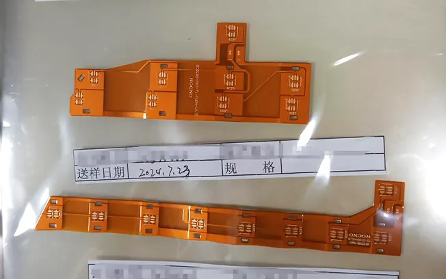
Figure 10 Product photo The flexible section is ultra-thin and unsupported
2. Technical Challenges
During flexible circuit board (FPC) area design, engineers incorporate connection points to support FPC production.
After completing cover removal, contour cutting, and testing, a “mold + laser cutting” process removes the connection points before board inspection.
This approach prevents the flexible area from jamming or creasing during production.
The specific process includes:
Pre-process → Milling the SET contour (retaining the FPC connection points) → Laser cutting 1 (flex circuit de-capping) → Remove protective tape → Remove film (remove residual adhesive from window hole rings) → Laser cutting 2 (laser-cut flex circuit outline, retaining connection points) → Nickel/gold plating → Electrical testing → Forming 1 (retaining flex circuit connection points) → Laser cutting 3 (cut flex circuit connection points) → Forming 2 (Milling the rigid board section at the connection points) → Post-processing.
A layer of protective tape covers the flexible board’s cover film before lamination to prevent adhesive residue and dust contamination.
This prevents adhesive overflow and powder shedding from the PP (without window openings) into the flexible area, which could affect quality and appearance;
We maintain the cleanroom temperature and humidity at 21°C and 50%, respectively, to prevent accelerated oxidation caused by excessive humidity and issues such as static-induced dust accumulation caused by excessive dryness.
After forming, use an air gun to blow away surface dust without passing the board through a washing line, thereby avoiding creasing in the flexible areas during washing.
Separate finished boards with paper after dust removal to prevent scratches and tangling.
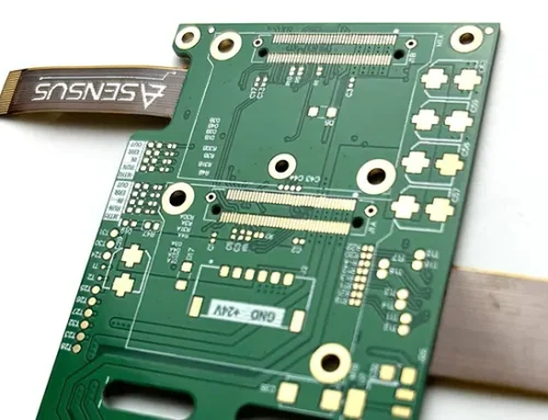
Product Manufacturing Results
Integration of all key technical aspects, along with coordination of the entire manufacturing process, enabled successful production of the expected product.
Figure 11 presents the physical product and its cross-sectional structure. The product passed all reliability tests; see Table 3 for details.

Figure 11 Actual product and cross-sectional structure
| No. | Test Item | Test Method | Acceptance Criteria | Test Result |
|---|---|---|---|---|
| 1 | Microsection Analysis | IPC-TM-650 2.1.1E—2004 | Copper plating thickness not less than 25.4 μm; dielectric layer thickness within specification requirements; no voids or cracks | Pass |
| 2 | Thermal Stress Test | IPC-TM-650 2.6.8—2004 | No blistering, delamination, board explosion, white spots, discoloration, or other defects | Pass |
| 3 | High Voltage Resistance Test | IPC-TM-650 2.5.7D—2004 | No arcing, discharge, or breakdown phenomena | Pass |
| 4 | Solderability Test | IPC J-STD-003B—2007 A1 | Area of poor solder coverage not greater than 5% of the single-sided pad area | Pass |
Table 3. Product Reliability Test Results
Conclusion
This paper uses a 10-layer, 3-stage stacked-via HDI rigid-flex PCB designed for portable medical electronic devices as an example.
The study provides a detailed overview of technical challenges in the manufacturing process. Cover removal and windowing require strict process control.
High-order blind and buried vias demand precise alignment accuracy. Laser-assisted plating plays an important role in blind-via fabrication.
The fabrication of the flexible section also presents significant technical difficulties.
Through systematic research and exploration, the engineering team successfully resolved these technical challenges. However, deeper exploration of technology and quality still requires the collective efforts of the entire industry.


