
Rigid-Flex PCB Structures and Process Flow: Common Configurations and Key Steps
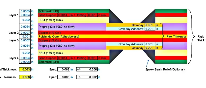

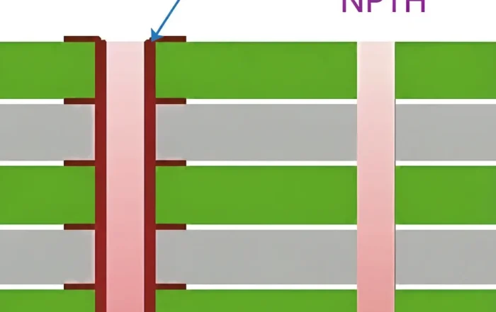
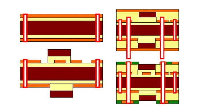
Additionally, a rigid-flex PCB bonds one or more rigid board sections to a flexible circuit substrate. Meanwhile, lamination, drilling and through-hole plating create the electrical links between layers. Therefore, the board bends where the product needs movement and stays stiff where components are soldered. For example, this guide explains rigid-flex PCB structures and process flow, from common stack-ups to the steps that build them.
What Defines a Rigid-Flex PCB Structure
In addition, a rigid-flex PCB, or R-FPCB, is a composite printed circuit board. As a result, a manufacturer combines a flexible PCB with a rigid PCB through lamination, following the relevant manufacturing requirements. The finished board therefore serves flexible and rigid areas at the same time.
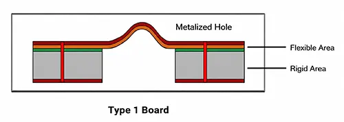
In practice, this structure saves internal product space and reduces the size of the finished product. In addition, it improves performance in products with special design and performance requirements. Next, for a wider view of the technology, read Rigid-Flex PCB Technology.
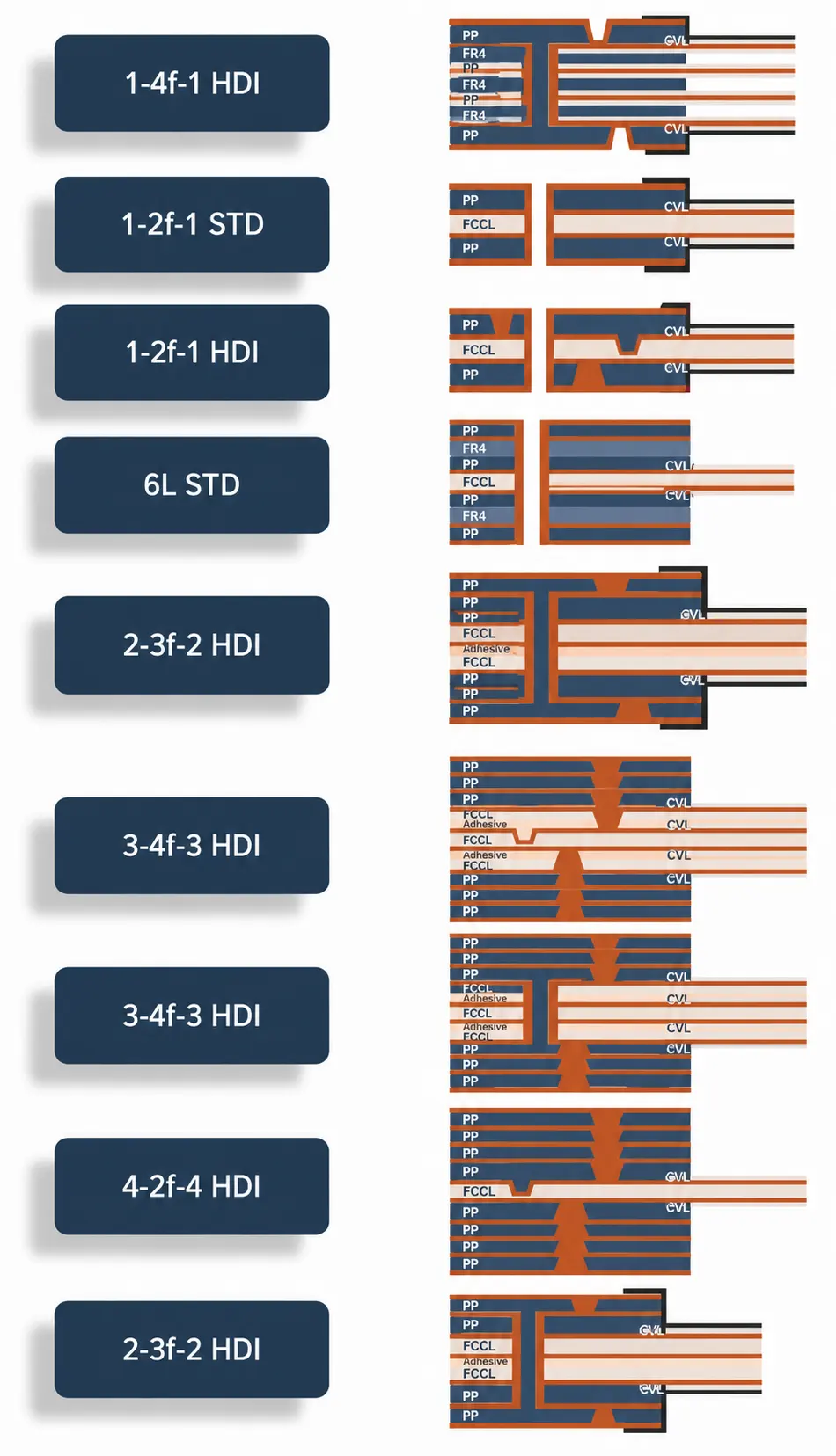
Rigid-Flex PCB Structures: Common Configurations
Layer Roles Inside the Stack
Consequently, four material groups carry the design: base film, bonding sheet, cover layer, and rigid core.
- Base film: polyimide film holds the conductors in every bending area.
- Bonding sheet: adhesive film joins flexible and rigid layers during PCB Lamination.
- Cover layer: coverlay or photoimageable coverlay shields flex traces from handling damage.
- Rigid core: stiff sections hold connectors, dense SMT, and large through-hole parts.
Moreover, the cover layer choice changes both the process route and the bend life, so it deserves its own comparison.
Base Film, Bonding Sheet and Cover Layer Compared
| Layer | Typical material | Role in the build | Selection points | Best suited to |
|---|---|---|---|---|
| Base film | Polyimide film with rolled or electrodeposited copper | Carries and supports the conductors in bending zones | Copper type, film thickness, dimensional stability after press | Dynamic bend areas, thin single- or double-sided flex cores |
| Bonding sheet | B-stage adhesive or no-flow prepreg | Bonds flex core to rigid layers and to cover layers | Resin flow, cure window, thickness tolerance, CTE match | Flex-to-rigid joints, air-gap builds where flow must stay local |
| Coverlay (adhesive coverlay) | Polyimide film plus adhesive, drilled or routed openings | Mechanical and electrical protection of flex traces | Opening tolerance, adhesive squeeze, registration to pads | General flex spans, larger openings, cost-sensitive builds |
| Photoimageable coverlay | Photo-defined polyimide-based resist | Protection with fine openings defined by exposure and development | Resolution, cure, adhesion after thermal cycling | Dense pad arrays, narrow openings, tight registration demands |
| Rigid core | FR-4 or similar rigid laminate | Stiffness, connector support, dense SMT and through-hole assembly | Tg, thickness, via capability, surface finish compatibility | Component zones, connector ends, edge stiffening |
In particular, adhesive coverlay is the workhorse for most flex spans because it is robust and easy to register to large openings. However, photoimageable coverlay wins where the opening geometry is finer than a routed coverlay can hold. Therefore, material grade affects bend life and cost, so fix the cover layer before tooling. Additionally, our overview of flex PCB materials covers how film, adhesive, and coverlay grades are selected.
Rigid-Flex PCB Stack-Up Configurations
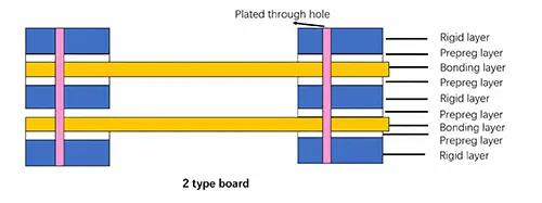
Meanwhile, rigid-flex PCB stack-up configurations follow two base rules. For example, a Type 1 board places one flexible board between several rigid boards. In addition, a Type 2 board joins several flexible plates with several rigid plates. As a result, derived structures then mix both ideas on one board.
Multilayer flexible cores are combined in the same way. A four-layer flexible circuit is built as 2+2, 1+2+1, or 1+1+1+1. Five-layer and six-layer flexible circuits reuse this combination method.
Around those cores, the usual build-ups are:
1. A single flex core with two rigid wings.
2. Symmetric double-sided flex, with equal copper and coverlay on both faces.
3. Asymmetric double-sided flex, with different copper weight per face.
4. Air-gap build, where the flex span stays unbonded between rigid areas.
5. Fully bonded build, where adhesive runs across the whole flex length.
6. Mixed multilayer build, with several rigid zones joined by flex cables.
7. Blind, buried, or stepped via build-ups inside the rigid zones.
Symmetric builds resist warp best. Air-gap builds bend freely, yet they need tight layer registration. Both trade-offs should be fixed before tooling starts. Our Rigid-Flex PCB page lists the build-ups we produce most often.
Reading a Build-Up Cross-Section
Read the stack from the outside in, and each layer maps to one process step. A typical single-flex-core build with two rigid wings, top to bottom:
| Position | Layer | Zone | Step that forms it |
|---|---|---|---|
| 1 | Outer copper of top rigid wing | Rigid only | Outer-layer imaging |
| 2 | Rigid core laminate | Rigid only | Material preparation and lamination |
| 3 | Bonding sheet | Rigid only, stops at flex window | Lamination (resin flow control) |
| 4 | Cover layer over flex copper | Flex span | Coverlay lamination |
| 5 | Flex copper and base film | Flex span | Inner-layer imaging and etch |
| 6 | Cover layer under flex copper | Flex span | Coverlay lamination |
| 7 | Bonding sheet | Rigid only, stops at flex window | Lamination |
| 8 | Rigid core laminate | Rigid only | Material preparation and lamination |
| 9 | Outer copper of bottom rigid wing | Rigid only | Outer-layer imaging |
Three consequences follow from this section view. First, the flex span carries no rigid core, so it must be protected by a cover layer on both faces. Second, the bonding sheet ends at the flex window, which is why resin flow control matters at that boundary. Third, every plated hole crosses the rigid zone only, so drill planning and desmear are decided by where the rigid cores sit. Air-gap variants leave positions 3 and 7 unbonded across the span, which removes adhesive from the bend but demands tighter registration of the flex outline.
Rigid-Flex Process Flow, Step by Step
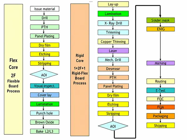
Rigid-Flex Process Flow
| Step | Action | Rigid-flex attention point |
|---|---|---|
| 1. Material preparation | Cut PI film, bonding sheet and rigid core | Match shrinkage across all materials |
| 2. Inner-layer imaging | Expose, develop and etch inner circuits | Check registration before press |
| 3. Lamination | Bond flex and rigid layers in one press cycle | Control resin flow at the flex window |
| 4. Drilling | Drill rigid zones and plated holes | Set entry and exit support on both faces |
| 5. Hole cleaning | Remove resin smear from hole walls | Use plasma desmear, not the aggressive chemical desmear used on rigid boards |
| 6. Copper plating | Plate hole walls and outer surfaces | Watch plating thickness near the flex joint |
| 7. Outer-layer imaging | Define outer circuits and lands | Keep bend areas free of heavy copper |
| 8. Coverlay and finish | Laminate coverlay, then apply final finish | Align coverlay to the flex outline |
| 9. Profiling | Route the outline and open the flex window | Cut cleanly at the rigid-flex boundary |
| 10. Electrical test | Verify nets before assembly | Test flex and rigid nets together |
Each press cycle fixes the final layer registration. As a result, drill accuracy and hole wall quality depend on lamination control. Flex-only variants of the same design run through the flexible core steps alone, which is why a Custom Flex PCB quote differs from a rigid-flex quote.
Comparing Standard PCB, Flex PCB and Rigid-Flex PCB
The three board families share imaging, etching and plating, then diverge. The table compares them on structure, process and cost behaviour.
| Attribute | Standard rigid PCB | Flexible PCB | Rigid-flex PCB |
|---|---|---|---|
| Layer structure | Rigid cores only, bonded with prepreg | Base film with copper, single or multilayer flex core | Rigid cores bonded to a flex core; rigid zones and bend zones on one board |
| Base material | Rigid laminate such as FR-4 | Polyimide film | Both, joined by bonding sheet |
| Cover layer | Solder mask | Coverlay or photoimageable coverlay | Coverlay on the flex span, solder mask on rigid zones |
| Stiffness | Stiff everywhere | Flexible everywhere | Stiff only where the rigid cores sit |
| Process route | Imaging, press, drill, plate, mask, finish | Flex core flow plus coverlay lamination | Flex core flow, then rigid lamination, then rigid-zone drilling and plating |
| Lamination cycles | One main press | One press, or an inner press for multilayer flex | Inner press plus final rigid-flex press, and possibly more for stepped builds |
| Hole cleaning | Standard chemical desmear | Short, gentle desmear | Plasma desmear to protect polyimide |
| Handling and panel support | Standard panels | Needs carrier or stiffener support | Needs support fixtures plus flex window protection |
| Bending capability | None | Full span | Only across the flex span |
| Relative unit cost | Lowest | Mid, rising with layer count | Highest, driven by press cycles and yield |
| Relative lead time | Shortest | Moderate | Longest |
| Typical use | Simple dense assemblies | Hinges, cables, moving parts | Assemblies that need both a stiff component zone and a moving hinge |
However, the cost gap follows from the process columns, not from the material alone. Two press cycles, a plasma desmear step, flex window profiling and fixture handling all add cost that a rigid board never pays.
How Design Rules Shape the Flow
Design rules decide which steps can hold tolerance.
- Bend radius: keep it large enough for the copper weight and the number of flex layers.
- Trace direction: run conductors perpendicular to the bend line to reduce fatigue.
- Vias: keep plated holes out of the bend region and place them in rigid zones.
- Transition zone: stagger coverlay ends and avoid conductor edges at the rigid-flex joint.
- Stiffeners: add local stiffeners under connectors instead of a full rigid layer.
When a design needs stiffness without a full rigid layer, Semi-Rigid Flex Printed Circuit Boards may offer a simpler route.
Acceptance Standards and Cost Drivers
Acceptance should be agreed before tooling, because a rigid-flex board cannot be reworked like a rigid board.
- Design stage: use IPC-2223 as the design reference for flex and rigid-flex, including bend radius, conductor orientation and cover layer rules.
- Performance stage: use IPC-6013 to qualify the finished flex and rigid-flex board, and the rigid-board reference for the stiff zones.
- Inspection scope: cover hole wall quality, cover layer adhesion, flex window cleanliness and dimensional registration at the rigid-flex boundary.
Cost drivers, in rough order of impact:
1. Number of press cycles and layer count in both the flex and rigid sections.
2. Build type: air-gap and stepped or blind via builds add steps and risk.
3. Panel utilisation, since flex material and rigid laminate are cut from different panels.
4. Cover layer type and opening resolution.
5. Test and fixture complexity for combined flex and rigid nets.
6. Volume, which absorbs set-up and press tooling across the run.
Defects, Yield and Cost Drivers
Rigid-flex boards involve a complex process that is difficult to execute, so yield is low. They also need large material and labor inputs. As a result, cost is higher and the production cycle is longer than for a rigid board.
Most process defects trace back to the steps above:
- Bubbles or voids after lamination, caused by moisture or trapped air.
- Resin squeeze-out into the flex window, driven by press flow.
- Hole wall cracks after drilling, linked to drill wear and desmear stress.
- Coverlay misregistration over exposed traces.
The advantages still balance these issues. Rigid-flex boards save internal space, shrink the finished product and improve performance in demanding designs.
FAQ
What is the difference between Type 1 and Type 2 rigid-flex configurations?
Type 1 combines one flexible board with several rigid boards. Type 2 combines several flexible plates with several rigid plates. Therefore, type 1 suits a single hinge or folded section. Type 2 suits designs with two or more separate bending areas. Derived structures extend both types with extra layers.
Which rigid-flex PCB stack-up configurations should I send for a quote?
Send a layer list for each zone, a map of rigid and flex areas, the coverlay type and the copper weight per layer. Add the bend location, surface finish and any stiffener. This detail lets the factory check symmetry, air gaps and via placement before tooling.
Is there a practical layer count limit?
There is no fixed ceiling, but practical limits come from the process rather than from the design software. Each added layer raises the number of press cycles and the registration stack, so a build that is easy at four to six total layers becomes a controlled operation at higher counts. Where a design needs more routing, splitting the rigid section into its own multilayer core and keeping the flex span thin is usually cheaper than pushing the flex core itself to a high layer count.
What bend radius should I design for?
Bend radius is set by copper weight, copper type and the number of flex layers, not by a single universal figure. As a working rule, thin polyimide flex with light rolled copper tolerates a much tighter radius than a multilayer flex core with heavier copper. Static bends can be tighter than dynamic ones that cycle repeatedly. State the bend type and cycle count on the drawing, then let the factory confirm the radius against the chosen build.
Should I specify coverlay or photoimageable coverlay?
Choose adhesive coverlay when openings are large, the build is cost-sensitive and routed or drilled windows can hold tolerance. Choose photoimageable coverlay when pad arrays are dense and openings are finer than a mechanical coverlay can register. Some builds mix both, using photoimageable coverlay on the fine-pitch span and adhesive coverlay elsewhere.
Why does a rigid-flex board cost more than a rigid PCB?
The process is complex and hard to control, so yield is lower. Material and labor inputs are higher as well. Together these factors raise unit cost and extend the production cycle. Symmetric builds and stable volume help reduce the gap.
Where can I check routine manufacturing questions?
Our PCB Manufacturing FAQ covers common process questions. For build-specific limits, send the stack-up to the factory before design freeze.
Related Posts
- Flex PCB Materials, Layup Structures, and Production Process — Related article
- Flexible PCB & Rigid Flex PCB Etching Process — Related article
- Manufacturing Process of Semi-Rigid Flex PCB — Related article
- PCB Lamination Process | Rigid & Flexible PCB Manufacturing Guide — Related article
- PI Protective Film Process for Rigid-Flex PCBs: Reducing Flexible-Area Cosmetic Defects – GekunFlex — Related article