
Conformal Nano Coating for PCB Protection: A Practical B2B Guide

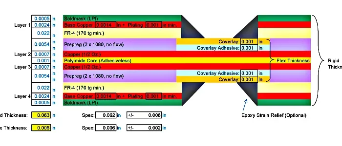
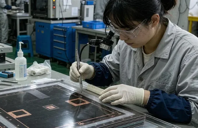

Therefore, conformal nano coating is an ultra-thin, usually 0.1–5 μm, protective surface treatment for PCBs. Additionally, it creates a hydrophobic barrier against moisture, condensation, and ionic contamination without the thickness or rework burden of traditional conformal coating. Meanwhile, it suits high-density and flexible assemblies where coating thickness, weight, and repairability matter.
In practice, engineers often encounter the term when evaluating a replacement for acrylic, silicone, or urethane conformal coating. Next, the comparison is not apples-to-apples. Consequently, a nano coating is a functional surface treatment; a traditional conformal coating is a protective coating system. Moreover, the right choice depends on exposure, assembly design, test strategy, and total cost.
What Is Conformal Nano Coating?
In particular, conformal nano coating forms a nanometre-scale film that follows the topography of the PCB. However, it lowers surface energy, so water beads and rolls off rather than spreading across the board. Therefore, the film is thin enough to leave connector mating, test points, and fine-pitch features largely unchanged.
Additionally, typical film thickness is 0.1–5 μm, depending on chemistry and process. Meanwhile, traditional conformal coatings are generally 25–250 μm thick. For example, that difference drives most of the tradeoffs: weight, thermal resistance, masking, cure time, and rework.
In addition, for flexible circuit boards, the low mass and thin profile help preserve bendability. However, flex assemblies still need careful handling and coverage validation. As a result, selection should start with Flexible coating materials, because not every nano chemistry is compatible with every solder mask, connector, or flex substrate.
Conformal Nano Coating vs Traditional Conformal Coating
In practice, use this table as a first screen, then validate with samples.
| Attribute | Conformal nano coating | Traditional conformal coating |
|---|---|---|
| Typical thickness | 0.1–5 μm | 25–250 μm |
| Protection mechanism | Hydrophobic surface barrier; low surface energy | Encapsulating film; physical and dielectric barrier |
| Moisture resistance | Good for condensation and splash; depends on IP target | Good to excellent; grade depends on chemistry and thickness |
| Abrasion resistance | Limited; not a wear layer | Better; silicone and urethane grades offer more toughness |
| Rework and repair | Often easier to clean and rework, but verify chemistry | More masking, stripping, and rework effort |
| Process | Spray, dip, or vacuum deposition; short cure | Spray, dip, brush, or selective robot; longer cure |
| Coverage | Excellent on high-density features; shadowing depends on process | Good, but thick films can bridge or fill fine gaps |
| Testing | Contact angle, IPX8, SIR, ionic contamination; post-coat test possible with care | Visual, thickness, dielectric, SIR, and adhesion tests |
| Best fit | Mobile, wearable, IoT, high-density PCBA | Harsh chemical, abrasion, long immersion, heavy-duty use |
| Main limitation | Thin film can be damaged by handling and abrasion | Thickness, masking, weight, and rework burden |
Next, the table shows why a simple price-per-litre comparison misleads. Consequently, nano coating uses very little material, but the process, masking, and validation determine the real cost. Moreover, also, the protection is not a thick physical cushion. If the board will see rubbing, sharp fixtures, or abrasive dust, a traditional coating may still be required.
Cost and Throughput Benchmarks by Scenario
The next screen is scenario-specific. In particular, the ranges below are starting points for a RFQ discussion, not guaranteed limits. However, confirm them with your coating supplier, application method, and test plan.
| Scenario | Typical protection target | Nano coating thickness target | Traditional coating thickness target | Relative material cost | Throughput consideration |
|---|---|---|---|---|---|
| High-density mobile or IoT with condensation and splash | IPX4–IPX7; SIR pass after thermal cycling | 0.1–3 μm | 25–75 μm acrylic or urethane | Low material use; higher cleaning and masking discipline | Selective spray and short cure support high-mix lines |
| Wearable or flex with bend areas | Splash and condensation; bend reliability | 0.1–3 μm | 25–50 μm | Low mass; rework-sensitive | Dip or spray with fixtures; validate bend coverage |
| Industrial or automotive splash and salt mist | IPX6–IPX7; salt mist and thermal cycling | 1–5 μm | 50–250 μm silicone or urethane | Medium; validation-heavy | Batch cure; masking and inspection time matter |
| Long immersion or abrasive contact | IPX8 only if full assembly qualified; abrasion resistance | Not usually the first choice | 100–250 μm | Higher material but more robust | Longer cure and harder rework reduce line throughput |
Therefore, throughput is driven by cleaning, masking, application, cure, and inspection—not by coating volume alone. Additionally, a nano line can run fast on selective spray, but it can lose time in surface preparation and coverage verification. Meanwhile, a thick-film line may use more material and longer cure, yet tolerate less precise cleaning in some processes. For example, compare boards per hour and first-pass yield on the same product family.
Where Conformal Nano Coating Fits in PCB Manufacturing
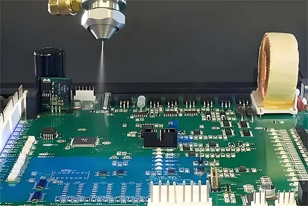
Conformal Nano Coating methods for spray
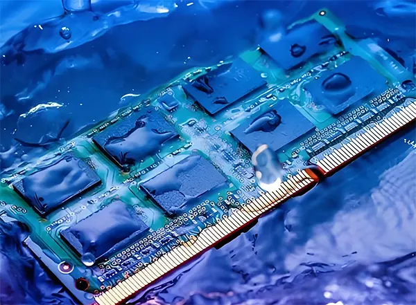
Conformal Nano Coating methods for dip
In addition, surface preparation is the first control point. As a result, cleaning PCB Boards before coating removes flux, oils, and particles that can cause dewetting or weak adhesion. For high-density flex, via quality and surface cleanliness matter; processes such as Dual-Laser Etching and
Cleaning for FCCL Blind Vias support consistent wetting and coverage.
Application methods include spray, dip, and vacuum deposition. Spray suits selective coverage and high-mix lines. Dip can give uniform coverage on complex shapes. Vacuum deposition supports conformal films on dense assemblies. In all cases, masking for connectors, test pads, and shielding must be defined before qualification.
Cure conditions need to match the chemistry. Some systems cure at room temperature; others need heat or UV. The process window should be fixed with the supplier, because under-cure can hurt durability and over-cure can affect solder mask or components.
Advanced assembly choices, such as Cutting-Edge 3D Steel Sheet Assembly Technology for Flexible designs, can change masking needs. Therefore, run a pilot with the actual stack-up, not a representative coupon only.
Performance and Test Methods That Matter
Qualification should reflect the field environment. Common checks include water contact angle, IPX8 or splash testing, salt mist, thermal cycling, ionic contamination, and surface insulation resistance. Contact angle is a useful process control, but it is not a stand-alone reliability proof.
Post-coating test access is a practical advantage. Some nano coatings allow electrical test after application, which can reduce handling risk. However, test probes can mark the film. The test plan should define probe locations, film repair, and accept/reject criteria.
Thermal performance also matters. Because the film is thin, it adds little thermal resistance. For power-heavy designs, pair the coating choice with FPCB heat dissipation planning rather than assuming the coating will solve heat problems.
Compliance, PFAS-Free Options, and Supply Chain Risk
Ask for RoHS and REACH declarations, SDS, and a PFAS-free statement if your market requires it. PFAS restrictions are evolving, so a coating that passed last year may need a new review. VOC content and local application rules can also affect line permits.
Sustainability teams increasingly review coating choices against Closed-Loop Recyclable Flexible PCB programs. A thin coating may reduce material use, but recyclability depends on removal, contamination, and end-of-life processing. Get written guidance before making a green claim.
Key Terms and How to Read a Coverage Diagram
Clear definitions reduce miscommunication in RFQs and test reports.
- Surface energy: the tendency of a liquid to spread on a solid. Low surface energy makes water bead and roll off.
- Contact angle: the angle where a water droplet meets the surface. A higher angle generally indicates a more hydrophobic surface.
- Dewetting: a coating defect where the film pulls away from the substrate, often caused by contamination or poor surface preparation.
- Shadowing: uneven coverage in recesses or under components because the coating flux cannot reach the surface.
- SIR (surface insulation resistance): a test that detects ionic contamination and electrochemical migration risk.
- Ionic contamination: conductive residues from flux, handling, or process chemicals that can cause leakage or corrosion.
- IPX8: an ingress protection rating for continuous immersion under defined conditions. It applies to the finished assembly, not the coating alone.
- PFAS: per- and polyfluoroalkyl substances. A PFAS-free claim needs a current supplier declaration.
A cross-section coverage diagram usually shows the PCB substrate, solder mask, components, and the coating film as a thin line. Read it by checking three things: whether the film follows edges and fine gaps, whether there are uncoated shadow zones under components, and whether the film thickness callout matches the process window. A top-down diagram may also show masking windows for connectors and test points. Treat the diagram as a process-control aid, not a guarantee of IP performance.
When Nano Coating Is the Right Choice — and When It Is Not
Choose conformal nano coating when the board is dense, thin, and exposed to condensation or splash. It fits mobile electronics, wearables, IoT sensors, and compact power modules. It also helps when masking windows are tight and rework access is limited.
Keep traditional conformal coating when the board faces abrasion, chemical attack, long immersion, or repeated mechanical stress. Silicone and urethane systems provide a thicker cushion and better wear resistance. High-voltage designs may also need the dielectric strength of a thicker film.
These tradeoffs sit alongside core challenges in manufacturing flex PCB, such as handling, dimensional stability, and yield. A coating decision that ignores those process realities will fail in production.
A Step-by-Step Selection Checklist
1. Define the environment: condensation, splash, salt mist, chemicals, abrasion, or immersion.
2. Set the protection target: IP rating, SIR limit, thermal cycling, and test method.
3. Review the assembly: density, connectors, shielding, test points, and flex bend areas.
4. Confirm rework and repair: strip method, probe access, and touch-up rules.
5. Validate the process: cleaning, masking, application, cure, and inspection.
6. Check compliance: RoHS, REACH, PFAS-free status, VOC, and customer-specific limits.
7. Compare total cost: material, yield, cycle time, rework, warranty, and field returns.
TCO: Why the Cheapest Coating Rarely Wins
Total cost of ownership includes more than material price. Nano coating often uses less material per board, but the cleaning, masking, and qualification effort can be significant. Traditional coating may cost less per litre, yet add thickness, cure time, and rework labor.
Build a TCO model with your actual yield data. Include rework rate, scrap, cycle time, energy, and warranty exposure. Then run a sample build. A coating that raises first-pass yield can justify a higher material price; a coating that causes touch-up rework cannot.
Use this comparison frame:
| Cost driver | What to compare | Why it changes the decision |
|---|---|---|
| Initial material | Grams per board and price per kilogram, not price per litre alone | Nano coating uses little material, so material price may be a small share of total cost |
| Yield | First-pass yield and dewetting or coverage rejects | Cleaning and wetting control often decide nano coating yield |
| Rework | Rework rate, touch-up time, and strip method | Easier rework can offset a higher material price |
| Warranty | RMA rate and field failure cost | A thin film that passes lab tests but fails in handling can raise warranty claims |
FAQ
What is conformal nano coating?
Conformal nano coating is an ultra-thin protective film, usually 0.1–5 μm, applied to a PCB to create a hydrophobic barrier. It resists moisture and ionic contamination while adding little thickness or weight.
Is nano coating better than traditional conformal coating?
Not universally. Nano coating suits high-density, thin, and rework-sensitive boards. Traditional conformal coating remains better for abrasion, chemicals, long immersion, and applications that need a thicker dielectric barrier.
What protection level can conformal nano coating provide?
Protection level depends on chemistry, film thickness, surface preparation, and the finished assembly. Many projects target IPX4–IPX7 for splash and condensation, with SIR and thermal cycling as supporting checks. IPX8 is possible only when the full enclosure, seams, connectors, and process are qualified. Specify the test method and pass criteria in the RFQ.
Can conformal nano coating achieve IPX8?
Some systems can support IPX8 when the full assembly, seams, connectors, and process are qualified. The rating belongs to the finished product, not the coating alone. Test the complete enclosure and PCB assembly.
Is nano coating PFAS-free?
Some suppliers offer PFAS-free formulations, but you must request a current declaration and SDS. Formulations change, and PFAS rules vary by market, so verify before production release.
Can coated boards be reworked?
Often yes, but the method depends on chemistry. Some films can be cleaned or locally repaired; others need controlled removal. Define probe access, repair limits, and touch-up materials before qualification.
Is conformal nano coating repairable at component level?
Component-level repair is often feasible, but it needs a defined procedure. Ask the supplier for a removal or touch-up method, then validate it on a sample board. Record whether the repair restores contact angle and passes the same SIR or splash test.
When should we not use nano coating?
Avoid it when the board faces abrasive wear, strong solvents, long immersion, or repeated mechanical stress. In those cases, a silicone, urethane, or other thick-film conformal coating is usually safer.
How do I compare quotes for conformal nano coating?
Ask each supplier to quote the same stack-up, masking scope, test plan, and acceptance criteria. Compare material usage, cleaning steps, cure time, rework rules, and warranty terms. A lower price per litre can hide extra inspection or field-return risk.
Next Step: Selection Guidance and Sample Request
Use the checklist above to shortlist two or three coating routes, then request samples on your actual stack-up. For a fast quote, send the PCB or flex build-up, target IP rating, exposure scenario, rework requirement, test plan, and expected annual volume. Ask for a PFAS-free declaration and a process window for cleaning, application, and cure. A sample trial is the fastest way to confirm coverage, cure, and total cost before production release.
Ready to evaluate conformal nano coating on your PCB or flex assembly? Send your stack-up, target IP rating, rework requirement, and test plan. A sample trial is the fastest way to confirm coverage, cure, and total cost.
Related Posts
- Flexible Coating Materials in Circuit Board Manufacturing – GekunFlex — Related article
- AI-Driven Optimization of Flexible Circuit Boards Production — Related article
- Boosting PCB and FPCB Heat Dissipation — Related article
- Cleaning PCB Boards — Related article
- Closed-Loop Recyclable Flexible PCB Manufacturing Guide — Related article