
Flexible Electronics Applications

Flexible electronics applications are product and process use cases where circuits, sensors, displays, lighting, or energy devices are built on bendable, conformable, or roll-to-roll-compatible substrates. The direct answer for selection is: match the application to bend radius, cycle life, thermal budget, barrier requirement, and inspection method before choosing materials; typical categories are flexible displays and sensors, wearable and medical patches, curved-surface human-machine interfaces, smart packaging, and lightweight sensing arrays. This page explains how those applications are evaluated and produced, with process checkpoints and scenario facts rather than brand claims.
Flexible electronics
See also Flex PCB Applications for related specifications.
See also FPC for Consumer Electronics for related specifications.
See also Automotive Flexible Circuit Boards for related specifications.
See also High-Reliability Flexible Circuits for High-End Applications for related specifications.
Quick answer: what makes an application “flexible electronics”?
A flexible electronics application is a design where at least one functional layer—conductive trace, sensor, display stack, or battery—must survive bending, folding, stretching, or conforming to a curved surface. Practical programs usually define four gates before tooling:
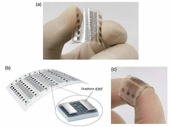
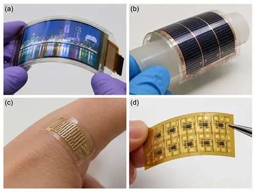
Figure 1: (a) Flexible gas sensor with an interdigital electrode structure fabricated on a PET substrate; (b) device structure diagram of a flexible field-effect transistor array based on graphene/carbon nanotubes; (c) optical photograph.
- Geometry gate: target bend radius and number of cycles.
- Thermal gate: maximum lamination, curing, and soldering temperatures the substrate and adhesive can take.
- Barrier gate: moisture and oxygen sensitivity of the active layer.
- Inspection gate: whether defects can be detected by optical, electrical, or roll-to-roll inspection at production speed.
If any gate is undefined, the application should stay in material screening rather than move to pilot lamination.
Flexible displays and sensors
Flexible displays and sensors are two of the clearest flexible electronics applications because they combine a bendable substrate with a patterned active layer and a protective stack. The production route usually follows: substrate cleaning → adhesive or planarization layer → electrode or backplane patterning → active-layer deposition → encapsulation → electrical test → bend and environmental reliability test.
Process checkpoints and typical target ranges to verify
| Checkpoint | Why it matters | Typical spec to confirm |
|---|---|---|
| Substrate thickness and CTE | Controls stiffness, warpage, and registration during lamination | Polyimide or PET-like films often evaluated in 25–125 µm range; CTE matched to process temperature |
| Transparent conductive layer | Balances conductivity with bending durability | Sheet resistance targets are application-specific; many touch and display programs start below 100 Ω/sq and then verify bend stability |
| Encapsulation barrier | Protects moisture-sensitive emitters or sensors | OLED-type stacks often target water vapor transmission rates below 10⁻⁴ g/m²/day; confirm by application |
| Bend test | Proves mechanical margin | Cyclic bend tests commonly start at 1–5 mm radius and 10,000–100,000 cycles, then inspect cracks and delta resistance |
| Inspection | Catches opens, shorts, delamination, and particles | Combine optical review with electrical continuity and, where relevant, roll-to-roll defect mapping |
For flexible displays, the main application decision is often backplane technology and encapsulation. For flexible sensors, the decision is usually electrode stability under repeated bending plus signal drift after humidity and temperature exposure. The same pilot line can support both, but the acceptance tests differ.
Flexible electronics use cases
Flexible electronics use cases span consumer, medical, industrial, and packaging scenarios. The useful way to compare them is not by product name but by the process constraint each one imposes.
Use case selection table
| Application scenario | Typical flexible format | Key process focus | Scenario fact to verify |
|---|---|---|---|
| Curved human-machine interfaces | Flexible touch film or printed electrode array | Lamination without air entrapment; trace registration on 3D surface | Surface curvature and adhesive thickness determine whether a 50–250 µm stack conforms without wrinkles |
| Wearable vital-sign patches | Stretchable or bendable sensor patch with conductive adhesive | Skin-contact lamination, sweat exposure, cyclic strain | Test at expected strain range and after simulated sweat exposure before claiming wear time |
| Medical disposable sensors | Screen-printed electrodes on flexible foil | Printing registration, drying and curing profile, sterilization compatibility | Confirm sterilization method does not degrade electrode or adhesive |
| Smart packaging labels | Printed antenna or sensor label on thin film | Roll-to-roll registration, die-cut tolerance, low-temperature curing | Read range and bend radius must be tested after converting, not only on flat sheet |
| Industrial curved-surface monitoring | Conformal sensor array or heater film | Adhesive selection, thermal cycling, connector strain relief | Verify signal stability after thermal cycling and repeated handling |
| Flexible lighting and signage | Encapsulated emissive film | Barrier lamination, edge sealing, defect inspection | Edge seal quality often limits lifetime more than the active area |
Differentiation case: conformal sensor array on a curved equipment surface
A practical differentiation example is a conformal sensor array for curved industrial equipment. The process starts with a flexible polyimide or PET carrier, then patterns an electrode array and routes it to a connector tab. The critical steps are: (1) define the bend radius from the equipment geometry, not from a flat coupon; (2) select an adhesive whose cure temperature stays below the substrate and sensor limits; (3) laminate under controlled pressure and vacuum to avoid trapped air; (4) strain-relieve the connector; and (5) inspect for micro-cracks after 10 thermal cycles and after the target bend cycles. This case matters because flat coupon examples often omit the connector and lamination steps that decide field yield.
How to evaluate a flexible electronics application before tooling
Use a four-stage screening process:
1. Material screen: compare substrate, adhesive, conductive layer, and barrier against thermal and bend requirements.
2. Coupon test: pattern a representative stack and run bend, humidity, and thermal cycling; record delta resistance, not just pass or fail.
3. Pilot lamination: move to the actual curvature, connector, and encapsulation; inspect for wrinkles, voids, and delamination.
4. Production inspection plan: define optical, electrical, and roll-to-roll checkpoints with sampling frequency and defect limits.
A program should not move from coupon to pilot if bend radius, cycle count, or barrier target is still to be confirmed. Those are the facts that determine whether a flexible electronics application is manufacturable.
FAQ
What are the most common flexible electronics applications?
The most common flexible electronics applications are flexible displays and sensors, wearable and medical patches, curved human-machine interfaces, smart packaging, conformal industrial sensing, and flexible lighting. The common thread is that at least one functional layer must survive bending or conforming.
What specifications should be defined first?
Define bend radius, bend cycle count, maximum process temperature, barrier requirement, and inspection method first. These five specifications determine substrate choice, adhesive choice, encapsulation, and whether roll-to-roll processing is realistic.
How do flexible displays and flexible sensors differ in process control?
Flexible displays usually place more emphasis on barrier encapsulation and defect-free backplane patterning. Flexible sensors place more emphasis on electrode stability, signal drift after humidity exposure, and connector strain relief. Both require bend testing and electrical inspection after lamination.
Related Posts
- Flexible PCB: Features, Design Guide & Applications — Related article
- Flex PCB Applications: Key Use Cases & Industries — Related article
- AI-Driven Optimization of Flexible Circuit Boards Production — Related article
- Cleaning PCB Boards — Related article
- Closed-Loop Recyclable Flexible PCB Manufacturing Guide — Related article