
Nickel–copper adhesion failure in flexible PCBs: causes, tests, and prevention
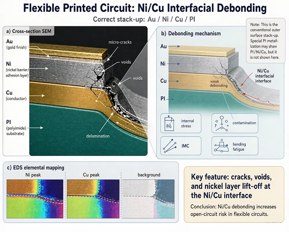
Nickel–copper adhesion failure is the loss of bond between a nickel plating layer and the underlying copper on a flexible PCB. It appears as blisters, peeling, a pink ring, or open circuits after thermal cycling, reflow, or bending. The main causes are copper oxide, organic contamination, weak microetch, and out-of-spec nickel bath chemistry—not the polyimide base film alone.
What nickel–copper adhesion failure looks like

Photograph of the location where the component fell off the failed sample
In a flexible circuit, the nickel layer acts as a diffusion barrier and solderable surface. When adhesion at the nickel–copper interface fails, you may see:
- Blisters or domes under the nickel/gold surface after reflow
- Edge peeling after micro-sectioning
- Pink ring around plated holes or pads
- Dark, brittle nickel with low peel strength
- Open circuits after dynamic bending
- Delamination during thermal shock or HAST
This is one of the most costly flexible PCB failure modes because it often passes visual inspection and only appears after SMT or in the field.
Root causes: surface, chemistry, and process
Nickel–copper adhesion is an interface problem, so every step that changes the copper surface or the nickel deposit matters.
| Category | Common cause | Field symptom |
|---|---|---|
| Copper surface | Oxide, organic residue, insufficient microetch, fingerprints | Blisters after reflow |
| Nickel bath | Low pH, high temperature, contamination, wrong current density, low agitation | Dark nickel, poor peel strength |
| Rinse and dry | Entrapped salts, water spots, incomplete drying | Localized peeling |
| Thermal | Excessive reflow, no post-plate anneal, CTE mismatch | Delamination after assembly |
| Mechanical | Tight bend radius at plated area, flexing during handling | Cracking at interface |
| Design | Plating over sharp copper steps, no teardrops | Stress concentration |
Copper surface preparation
Copper oxide is the most common cause. If the copper is not perfectly clean and oxide-free before nickel plating, the nickel bonds to oxide rather than to copper. The oxide layer then fails under thermal or mechanical stress. Proper steps include alkaline cleaning, acid activation, and controlled microetch. Microetch removes 0.5–1.5 µm of copper and leaves a uniform, active surface. Over-etching creates a rough surface that can trap chemistry; under-etching leaves oxide.
Nickel plating chemistry
Nickel sulfamate baths are common for flexible circuits because they produce low-stress deposits. Key controls:
- pH 3.5–4.5
- Temperature 45–55 °C
- Current density 2–5 A/dm²
- Continuous filtration (1–5 µm)
- Carbon treatment when organic contamination is suspected
- Stress reducer at the correct concentration
If pH is too low, hydrogen evolution increases, and adhesion suffers. If pH is too high, nickel hydroxide can form. Contamination by copper, iron, or organics can also cause dark, stressed deposits.
Rinsing and drying
Nickel bath drag-out must be rinsed thoroughly before gold or other subsequent steps. Entrapped salts and water spots create local adhesion failures. Use cascading rinses and DI water with controlled conductivity.
Thermal and mechanical stress
Even a good interface can fail if the finished flexible circuit is bent too tightly at a plated pad or if reflow exceeds the material limit. Post-plating annealing at 150–180 °C for 1–2 hours can relieve stress and improve adhesion, but it must be compatible with the base film and coverlay.
How to diagnose nickel–copper adhesion failure
Use a combination of tests:
1. Tape test (ASTM D3359) – quick check for poor adhesion on plated surfaces.
2. Peel test (IPC-TM-650 2.4.9) – quantitative peel strength for plated copper.
3. Cross-section – inspect the nickel–copper interface for voids, oxide, or separation.
4. SEM/EDS – identify oxide, phosphorus-rich nickel (black pad), or contamination.
5. Thermal shock (IPC-TM-650 2.6.7) – cycling to reveal latent failures.
6. Bend test – simulate dynamic flexing at the plated area.
For nickel-gold plated FPC adhesion failure, black pad is a related but distinct mechanism: excessive nickel corrosion during immersion gold creates a phosphorus-rich surface that is brittle and poorly solderable. Cross-section and EDS are the reliable way to separate black pad from simple oxide-related nickel–copper adhesion failure.
Prevention: process controls that work
1. Control incoming copper foil and FCCL
Use consistent RA or ED copper foil with known surface treatment. Store FCCL in clean, dry conditions. Do not use material beyond shelf life.
2. Lock the pre-plating clean and microetch
- Alkaline clean, rinse
- Acid activation, rinse
- Microetch to 0.5–1.5 µm, rinse
- DI rinse and dry
Monitor microetch rate weekly. Replace baths based on copper concentration, not only time.
3. Maintain the nickel bath within a tight window
Use automatic dosing for pH and temperature. Analyze bath samples for nickel, copper, iron, and organics. Filter continuously and carbon treat on a schedule.
4. Anneal after plating when the application requires it
For dynamic-flex or high-reliability builds, anneal at 150–180 °C for 1–2 hours in an inert atmosphere if the coverlay and adhesive system allow. Verify adhesion before and after annealing.
5. Design for the plating interface
Avoid placing plated pads at the tightest bend radius. Use teardrops, anchor tabs, and gradual transitions. If the design must bend near a plated area, choose a material system with a proven dynamic bend rating—see how to choose flex material.
Applications where nickel–copper adhesion failure matters most
- Display FPC: fine lines and repeated bending make interface defects visible as line noise or open circuits. See display FPC.
- Automotive: thermal cycling, vibration, and high reliability requirements. See Automotive Flexible Circuit Boards.
- Medical and industrial: long-term reliability and sterilization cycles.
- Consumer electronics: reflow and drop performance.
Why Gekun controls nickel–copper adhesion
Gekun is a flexible PCB manufacturer focused on Flexible Circuit and Flex PCB Assembly for demanding applications. Our process controls include:
- Incoming material verification
- Controlled microetch and nickel bath analysis
- Peel testing and cross-section inspection
- Thermal shock and bend testing
- Full traceability from FCCL lot to finished FPC
We support Our Markets with engineering reviews, stack-up optimization, and failure analysis. If you are seeing blisters, peeling, or open circuits after assembly, send us your stack-up, plating specification, and failed samples. We will help isolate whether the root cause is surface preparation, nickel chemistry, thermal stress, or design.
Request a manufacturing review or ask for a sample build with controlled nickel–copper adhesion.
FAQ
Q: What causes nickel–copper adhesion failure in flexible PCBs?
A: The most common causes are copper oxide before plating, organic contamination, insufficient microetch, and out-of-spec nickel bath chemistry (pH, temperature, current density, contamination). Thermal stress and bending can then turn a weak interface into a visible failure.
Q: How do you test nickel–copper adhesion on an FPC?
A: Use the tape test ASTM D3359 for a quick check, the peel test IPC-TM-650 2.4.9 for quantitative data, cross-sectioning for interface inspection, SEM/EDS for contamination or black pad, and thermal shock or bend testing for latent defects.
Q: Is nickel–copper adhesion failure the same as black pad?
A: No. Black pad is a specific failure after immersion gold where the nickel surface becomes phosphorus-rich and brittle. Nickel–copper adhesion failure is the broader loss of bond between nickel and copper, which can be caused by oxide, contamination, or bath issues without black pad.
Q: Can nickel–copper adhesion failure be fixed after assembly?
A: Usually no. Once the interface has blistered or peeled, rework is risky and often not reliable. The correct approach is to identify the root cause in the plating process, qualify a corrected build, and validate with peel, thermal shock, and bend tests.
Q: What plating controls prevent nickel–copper adhesion failure?
A: Control copper surface preparation (clean, activate, microetch 0.5–1.5 µm), maintain nickel sulfamate bath at pH 3.5–4.5, 45–55 °C, 2–5 A/dm², filter continuously, carbon treat when needed, rinse thoroughly, and anneal at 150–180 °C for 1–2 hours when the application requires it.
Q: Does bending cause nickel–copper adhesion failure?
A: Bending can reveal or accelerate a weak nickel–copper interface, especially if plated pads are placed at a tight bend radius. It is rarely the only cause; oxide, contamination, or stressed nickel deposits usually set the stage.
Related Posts
- Nickel-Gold Plated FPC Boards — Related article
- Flexible PCB Failure Modes & Prevention Guide — Related article
- Right Flex Material — Related article
- FPCB Differential Impedance Optimization with Mesh Copper — Related article
- PCB Copper Plating Process — Related article