PI-Based Flexible Circuits: 3D Printing Encapsulation and Liquid Metal Reliability Optimization (Part I)

Flexible circuits have been a hot topic in recent years in the fields of health monitoring, biomedicine, and rehabilitation diagnostics. Manufacturers fabricate traditional flexible conductors by combining conductive fillers with stretchable elastomers.
Introduction
For example, embedding nano-metal particles and ionic gels into an elastomer forms conductive elastomers capable of withstanding complex strain conditions;
however, humidity and temperature significantly affect the electrical conductivity of these conductive elastomers, leading to unstable conductivity.
Liquid Metal as an Emerging Solution
In recent years, liquid metals have seen widespread use as circuit materials for flexible electronic devices.
The primary constituent of liquid metals is eutectic gallium-indium alloy, which remains liquid at room temperature.
This liquid metal exhibits excellent and consistent electrical and thermal conductivity, a low melting point (<30 °C), non-toxicity, and unique surface chemical properties.
As a soft conductive material with excellent performance and stable properties, liquid metal holds immense potential for flexible wearable devices and soft robotics.
Encapsulation Challenges in Flexible Circuits
The key to fabricating liquid-metal-based flexible electronic devices lies in the precise encapsulation of the circuits.
PDMS and Ecoflex commonly serve as encapsulation materials for circuits. Although they offer good flexibility and tensile properties, the encapsulation layer and substrate layer of these two materials do not bond well, making them prone to cracking.
This requires methods such as plasma treatment to strengthen the bond; however, plasma treatment causes some damage to the material, reducing its mechanical strength.
Advantages of PI for Integrated Encapsulation
During the printing process, the substrate layer and encapsulation layer of PI can fuse and bond with each other, thereby achieving tight encapsulation of the circuit.
Furthermore, compared to PDMS and Ecoflex, PI possesses superior mechanical and dielectric properties, as well as excellent temperature resistance.
Therefore, this paper proposes using PI as both the substrate and encapsulation material for flexible circuits to achieve integrated molding.
Limitations of Traditional Encapsulation Methods
In traditional surface encapsulation processes, excessive use of PI solution during circuit encapsulation can cause the organic solvents in the solution to dissolve the partially iminated PI substrate.
Although this dissolution promotes the integration of the substrate with the encapsulation layer, excessive dissolution of the PI substrate significantly weakens its original mechanical strength and structural integrity, rendering it unable to support the circuit.
This leads to circuit sagging and leakage, severely compromising the reliability and stability of the encapsulation.
Proposed 3D Printing Encapsulation Strategy
This study introduces a novel 3D printing technology for the encapsulation of flexible liquid metal circuits based on a PI substrate.
By regulating the line width of the encapsulation layer and the degree of imidization of the substrate, this technology ensures effective integration between the substrate and the encapsulation layer, effectively preventing circuit settlement and leakage caused by excessive dissolution.
This improvement enhances the integrity and tightness of the circuit encapsulation, providing a robust guarantee for the stable operation of the circuit.
Controlling the curing temperature and time adjusts the imidization degree of the PI substrate, regulates the degree of substrate dissolution, and thereby controls the extent of liquid metal sedimentation.
This method not only opens up new avenues for optimizing circuit encapsulation technology but also enhances the reliability of circuit encapsulation.
Experimental Section
Main Materials
Thermosetting PI, SG1020, Dongguan ZhanYang Teflon Co., Ltd.; Liquid Metal, DG-19, Dongguan Dingguan Metal Technology Co., Ltd.
Major Equipment and Instruments
Confocal Laser Microscope (CLM), VK-X1050, Keyence Corporation;
Vacuum Oven, DZF-6050, Shanghai Yiheng Scientific Instruments Co., Ltd.;
Scanning Electron Microscope (SEM), JEOL JSM-5900LV, JEOL Trading Co., Ltd.;
Optical Microscope, S750, Meishidi Dongguan Technology Co., Ltd.;
Electron Microscope, DM401, Shenzhen Yong’an Technology Co., Ltd.; Bending and Torsion Tester, QL-5E, Xiamen Meide Electronic Technology Co., Ltd.;
Resistance Tester, RK2518-32, Shenzhen Meirui Electronic Technology Co., Ltd.
Sample Preparation
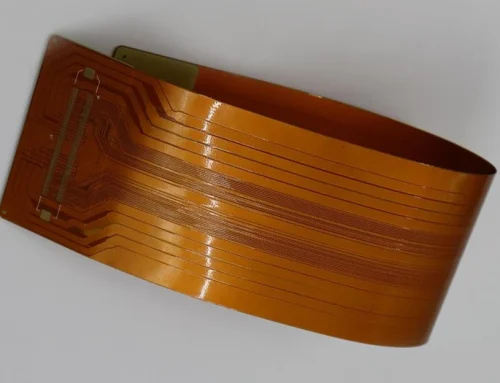
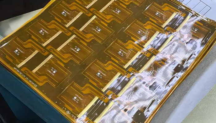
Figure 1 shows the flexible circuit sample preparation process. The specific process steps are as follows:
Step 1: Pre-treat the glass substrate. Clean the glass substrate with anhydrous ethanol, then dry it in a vacuum oven at 80 °C for 5 minutes. Align and adhere the glass substrate to the printing substrate.
Step 2: Print the PI base layer. Set appropriate flow rate and cycle parameters to ensure the formation of an ideal liquid film morphology.
Step 3: Cure the PI base layer. Perform isothermal curing under strictly controlled temperature and time conditions to achieve the desired degree of imidization and surface morphology.
Step 4: Print the circuit. After adjusting the printing parameters, activate the electrohydrodynamic jet 3D printing equipment to print the liquid metal material, thereby completing the fabrication of the flexible circuit.
Step 5: Print the PI encapsulation layer. Set appropriate flow rate, speed, and voltage to print the PI imide encapsulation layer onto the circuit.
Step 6: Cure the encapsulation layer. Perform isothermal curing under strictly controlled temperature and time conditions to ensure uniform shrinkage of the encapsulation layer and maintain the circuit’s morphology.

Fig. 1 Flexible circuit sample preparation process
Basic Technical Principles
In flexible circuit fabrication, direct-to-material writing technology prints the PI substrate layer.
As shown in Figure 2, the combined effects of back pressure and gravity force the liquid to overcome viscous forces and surface tension and extrude from the nozzle as a droplet, which then deposits precisely onto the substrate.
As shown in Figure 3, an electrohydrodynamic jet method prints the circuit and encapsulation layers. The process holds the nozzle vertically downward to stabilize the jet.
The power supply connects its positive terminal to the nozzle and its negative terminal to the substrate, creating a strong electric field.
The electric field causes the liquid at the nozzle tip to accumulate a charge, gradually forming a Taylor cone.
When the electric field strength is sufficiently high, the electric field force overcomes the liquid’s surface tension and viscosity, forming a fine jet.
As the jet moves, it splits into tiny droplets, which eventually deposit onto the substrate to form the desired circuit or encapsulation layer.
Surface Encapsulation: Sedimentation and Leakage Mechanism
Figure 4 illustrates the sedimentation and leakage process of the circuit under surface encapsulation, as well as the cross-sectional morphology of the circuit after thermal curing.
Initially, the liquid metal circuit is precisely printed onto the PI substrate [Figure 4(a)]. Subsequently, surface encapsulation is performed and the substrate is heated [Fig. 4(b)].
The PI substrate is then rapidly softened and eventually completely dissolved by an excess of solvent molecules, causing the circuit to sink rapidly [Fig. 4(c)].
Ultimately, the liquid metal begins to leak out of the substrate layer [Fig. 4(d)], threatening the integrity and stability of the flexible circuit.
After thermal curing, the dissolution process stops, and the circuit’s sinking and leakage cease [Fig. 4(e)].
Fig. 4(f) is an SEM image showing the cross-sectional morphology of the circuit under surface encapsulation.
Wire Encapsulation Strategy for Controlled Sedimentation
Fig. 5 illustrates the sinking process of the circuit under wire encapsulation and the cross-sectional morphology of the circuit after thermal curing.
The process initially prints the liquid metal circuit onto a PI substrate [Fig. 5(a)].
Subsequently, the process encapsulates the wires and heats the sample [Fig. 5(b)].
Next, immersion in an appropriate amount of solvent molecules softens and dissolves the PI substrate [Fig. 5(c)].
The wire encapsulation ensures the encapsulation of a precise volume of PI solution, facilitating the controlled sedimentation of the circuit and the integration of the substrate with the encapsulation layer.
Once the solvent molecules are exhausted, the substrate stops softening and dissolving, and the circuit stops sedimenting.
The circuit’s position remains largely fixed, while the PI substrate remains uncured [Fig. 5(d)]. After final thermal curing, the liquid metal fixes in place and forms a stable circuit structure [Fig. 5(e)].
Figure 5(f) shows the cross-sectional morphology of the circuit under the encapsulation layer.
Key Mechanism of Process Control
The key to the wire encapsulation technique lies in regulating the line width of the liquid PI encapsulation layer to control substrate dissolution and, consequently, circuit deposition.
This lays the foundation for further regulating circuit deposition by controlling the degree of imidization of the PI substrate in subsequent steps.

Fig. 2 Material direct writing printing principle

Fig. 3 Printing principle of electrohydrodynamic injection

Fig.4 Sedimentation leakage process of the circuit under surface

Fig. 5 The sedimentation process of the circuit in wire package
Results and Discussion
Control of Circuit Sedimentation
A comparison of circuit sedimentation before and after treatment is shown in Figure 6.
The degree of imidization of the PI substrate layer and the amount of encapsulation layer used are critical factors affecting the settlement of liquid metal circuits.
Therefore, we investigated the influence of the substrate curing process (heating temperature and time) and the line width of the encapsulation layer on circuit settlement (Figure 7).
To control the variables, the circuit line width was standardized at 150 (±5) μm.

Fig. 6 Comparison before and after circuit settlement

Fig. 7 Influence of process parameters on circuit settlement rate
Sedimentation Rate Calculation
The formula for calculating the settlement rate is defined as:

Formula 1
In the equation:
- H — sedimentation rate, %
- h1 — initial height, μm, as shown in Figure 6(a)
- h2 — final height after sedimentation, μm, as shown in Figure 6(b)
Effect of Curing Temperature and Time
Figures 7(a) and (b) illustrate the effects of heating temperature and heating time on circuit settlement for the PI substrate layer.
The encapsulation layer has a line width of 2 mm. At a heating time of 6 h, as the temperature increased from 40 °C to 80 °C, the settlement rate decreased from 85% to 8%; at 60 °C, as the heating time increased from 4 h to 8 h, the circuit settlement rate decreased from 86% to 23%.
This indicates that as heating time and temperature increase, the thermal imidization of the substrate layer becomes more complete, the structure becomes more stable, the supporting force for the circuit is enhanced, and the settlement rate decreases.
Effect of Encapsulation Line Width
Figure 7(c) reveals the relationship between the line width of the encapsulation layer and circuit settlement. Under conditions of 60 °C and 6 h, as the line width increased from 1.0 mm to 3.00 mm, the circuit settlement rate rose from 12% to 49%.
A wider line width implies a greater amount of PI solution used during encapsulation, which enhances the solution’s dissolving effect on the substrate layer.
This causes the substrate structure to become more porous, weakening its support for the circuit and consequently increasing the settlement rate.
Optimization Outcome
Figure 7(d) shows the surface morphology of the circuit settlement under SEM imaging.
Controlling the circuit settlement rate to a minimum of 8% demonstrates that the performance and quality of circuit encapsulation can be significantly improved through appropriate process optimization.
Effect of Process Parameters on the Thickness and Surface Roughness of the PI Substrate Layer
The thickness and surface roughness of the PI substrate layer directly affect the print quality of the circuit as well as the comfort and thinness of the device.
To ensure stable formation of the PI substrate layer and high-quality printing, it is necessary to investigate the effects of print flow rate and cycle time on the substrate layer thickness and surface roughness (Figure 8).
By exploring these printing parameters, the conditions for printing high-quality PI substrate layers can be determined.
Figure 8(a) shows that thickness increases with increasing print flow rate (300–700 μL/min); an appropriate flow rate ensures continuous and stable printing of the substrate as well as surface smoothness.
Figure 8(b) illustrates the effect of cycle length (1–5 mm) on thickness. The results indicate that increasing the cycle length leads to a decrease in thickness.
When the cycle length exceeds 5 mm, print continuity is compromised, the solution fails to level properly, and a smooth film surface cannot be formed.

Fig. 8 Influence of process parameters on the thickness of PI
Surface Formation Mechanism
The surface roughness of the PI substrate is a key indicator of print quality and is significantly influenced by the printing cycle and flow rate.
During printing, as shown in Figure 9, liquid PI fuses along the grid lines to form a surface.

Fig. 9 Film formation principle of liquid PI base layer
Effect of Printing Cycle on Surface Roughness
As shown in Figure 10, this study investigated the effects of a print flow rate of 500 μL/min and print cycles (1–5 mm) on the surface roughness of the PI substrate layer.
Figure 10 (a) through (e) shows the CLM scan morphologies of the substrate layer at different print cycles. As shown in Figure 10(f), surface roughness gradually increases as the print cycle lengthens.
An increase in the printing cycle leads to a widening of the line spacing.
If the solution’s flowability is insufficient to bridge the increased spacing, it will result in difficulty in leveling the liquid film, thereby increasing surface roughness.

Fig. 10 Influence of printing cycle on surface roughness of PI base layer
Effect of Flow Rate on Surface Roughness
As shown in Figure 11, the effects of a print cycle of 3 mm and print flow rates ranging from 300 to 700 μL/min on the surface roughness of the PI substrate layer were investigated.
Figure 11(a)–(e) shows the CLM scan morphologies of the substrate layer at different print cycles. As shown in Figure 11(f), surface roughness gradually increases as the print flow rate increases.
This effect is most pronounced at 700 μL/min; the color contrast in the CLM scan image in Figure 11(e) is the most striking, intuitively reflecting the significant increase in the surface roughness of the substrate layer.
Excessively high print flow rates cause the liquid film thickness to increase abnormally, leading to uneven shrinkage during the heating and curing process, which in turn increases roughness.

Fig. 11 Influence of print flow on surface roughness of PI base
Continue reading: Part II