Medical Ultrasound FPCB Design: Optimization of 3L Stepped and Cutout Flexible Circuit Structures
Ultrasound probe products are widely used in medical diagnostic equipment. Some probes are designed for single use and are classified as medical consumables, resulting in strong market demand and broad growth prospects.
Development Trends of FPC in Medical Ultrasound Devices
The development of flexible printed circuit (FPC) boards for medical ultrasound products is mainly characterized by:
- Miniaturization
- High wiring density
- High interconnectivity
- Enhanced structural strength
- Efficient heat dissipation
- Ease of assembly
At present, leading medical customers are proposing new requirements for compact medical ultrasound FPCB designs with specialized structures.
These designs represent an inevitable trend toward miniaturization and high-density integration in ultrasound devices.
The market potential for such products is significant, especially in Europe and the United States.
However, existing manufacturing capabilities and process solutions are currently insufficient to support these specialized FPC structures.
Advantages of Stepped FPC Structure Design
In traditional PCB designs, all components are arranged on the same plane, which can lead to interference between components or insufficient layout space. The stepped FPC structure effectively addresses these issues by improving spatial arrangement and reducing interference.
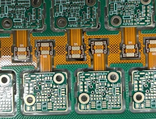
Single-Sided Hollow Finger FPC Design
For single-sided hollow FPC boards, the finger pattern in the hollow area maintains high flatness. The combination of hollowing and routed finger separation results in low deformation, meeting the design requirements for connections at both ends and improving overall product reliability.
Process Solutions for 3L Stepped FPC
Based on these requirements, two technical approaches are studied for 3-layer (3L) stepped FPC boards:
- Using screen-printed solder mask with peelable adhesive
- Applying carrier film lamination combined with controlled-depth coverlay removal
These methods evaluate the feasibility of product structures under different processes and improve manufacturing yield while resolving wrinkling defects in stepped areas.
Process Development for Single-Sided Hollow FPC
To establish technical capability for single-sided hollow boards and prevent finger cracking or bending in hollow areas, two process routes are developed:
- Polyimide (PI) windowing before copper lamination, followed by dry film application on circuit areas and anti-plating dry film protection on finger areas
- PI windowing after etching, followed by coverlay lamination and anti-plating dry film protection on finger areas
Technical Achievements
This study resolves key issues such as wrinkling in critical areas of 3L pure flexible stepped boards and validates manufacturing processes for hollow FPC structures. It expands the technical scope of medical ultrasound FPC applications and establishes a foundation for future development and production of such specialized structures.
Experimental Section
Mechanism Analysis and Experimental Design of 3L Stepped Flexible Circuits
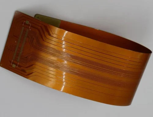
The 3L pure flexible board step board has a thickness of 0.14 mm. The product structure is shown in Figure 1(a). The dark central step area is designed with 6 μm copper foil, and the step width is 4.7 mm.
The structure of this central step area consists of a 6μm thin copper layer without any supporting structure.
It has poor resistance to deformation and is prone to edge warping caused by the negative pressure during vacuum lamination and the compressive stress from the press, resulting in product scrap;
As shown in the stress simulations in Figures 1(b) and 1(c), the asymmetric laminate structure, along with the design of internal vent holes and resin channels, creates areas of high stress concentration in critical regions.
Therefore, the primary cause of wrinkling is the lack of structural support in these critical areas, which leads to deformation under stress.

Figure 1: Step Structure and Stress Analysis
The feasibility of forming 3L stepped flexible circuits was verified through the following three technical approaches to address creasing defects in critical areas.
Technical solutions
As shown in the technical solutions in Figure 2:
Solution A:
- Form the steps first, then laminate.
- mill grooves on the solder surfaces L3 and L4;
- screen-print a peelable adhesive to provide a support structure;
- After electroplating, remove the film and clean the peelable adhesive.
Solution B:
Laminate first, then perform controlled-depth milling of the step.
A peel-off cover method applies a load-bearing film to critical areas on the TOP side and high-temperature tape to Layer L2.
The process removes the peel-off cover at a controlled depth after electroplating but before contouring.
Solution C:
Replace red copper with high-strength titanium-copper (TiCu) or beryllium-copper (BeCu).
Although this option is more costly, it serves as a backup solution.

Figure 2: 3L step flexible substrate technology roadmap
Specific Design Plan for Screen-Printing Peelable Adhesive:
- Mill grooves on the core boards of layers L3 and L4; screen-print the peelable adhesive (yellow peelable PI adhesive###) twice on layer L2 of the layer 101 core board;
- The width of the peelable adhesive should be 0.20 mm narrower on one side than the step area.
- Add a laser-cut outline to the outer layers.
- After electroplating, add a film removal process to remove the peelable adhesive.
The theoretical milling groove depth is 71 μm, so two screen prints match the groove depth.
Screen printing parameters for the peelable adhesive: printing speed 10 cm/s, mesh count 41T, wet film thickness 40–45 μm.
Specific design for depth-controlled peel-off:
- Apply a carrier film to the critical areas on the top surface of Layer 101, extending at least 1.0 mm beyond the step region on each side for support.
- apply high-temperature tape to Layer L2 (###);
- After the first laser contouring on Layer 000, add a UV depth-control process on the solder side (performing depth control and opening on two edges within the board), followed by peel-off.
- Add a carrier film removal process after electrical testing, but before contouring.
Mechanism Analysis and Experimental Design of Single-Sided Perforated Flexible Circuit Boards
Figure 3 shows the structural design of the perforated board. The board thickness is 0.18 mm, with product dimensions of 64.26 × 40.18 mm.
The perforated finger dimensions are 0.736 ± 0.1 mm × 0.2 ± 0.05 mm. The PI thickness is 50 μm, and the copper thickness is ≥35 μm.
The fingers in the perforated area are prone to breaking or bending, making it difficult to ensure positional accuracy.
Since the perforated finger area lacks support and structural reinforcement, the forming process and machining operations likely cause finger fractures or bending.
Therefore, two process routes provide solutions: one cuts the PI window with a laser before circuit fabrication, and the other fabricates the circuit before laser cutting the PI window.
This ensures that the open-frame fingers do not break or bend, verifies the feasibility and quality performance of the manufacturing process, and determines the optimal process route for the open-frame finger FPC product.

Figure 3: Close-up view of the finger area
Based on research and analysis, two technical approaches for producing single-sided perforated boards, as shown in Figure 4, prove feasible.
We will establish the manufacturing capabilities for perforated board products and verify the feasibility of the processes:
(1) PI windowing first + pure adhesive + copper foil process;
(2) Single-sided FCCL etching followed by PI windowing.

Figure 4: Manufacturing Process for Single-Sided Perforated Flexible Circuit Boards
Testing Methods
The testing methods are shown in Table 1.
Appearance-related inspections are conducted using a microscope, while dimensional inspections are performed using a coordinate measuring machine (CMM) with a sampling rate of 20%.
| Category | Item | Test Method | Inspection Frequency | Standard Requirement |
|---|---|---|---|---|
| Step Board | Key Area Warpage | Final Inspection | 100% Inspection | No warpage in key areas |
| Dimensional Characteristics | Microscope | 20% Sampling per Batch | According to drawing standard | |
| Hollow Board | Appearance | Final Inspection | 100% Inspection | No warpage in key areas |
| Hollow Position Accuracy & Dimensional Accuracy | CMM (Coordinate Measuring Machine) | 20% Sampling per Batch | CPK ≥ 1.33 |
Table 1: Experimental Testing Methods
Experimental Results and Analysis
Results and Analysis of the 3L Step Plate Experiment
The processing results for the step regions of the samples are shown in Table 2.
For the screen-printed peelable adhesive scheme, the acceptance yield for critical areas was 83.16%, with a process yield loss of 4%.
For the peel-off + carrier film application scheme, the process yield for critical areas was 97.44%, the acceptance yield was 94.23%, and the process yield loss was 3% (NG: Non-conforming products, Y: Conforming products).
| Category | Process Stage | Sample Quantity (pcs) | Qualified Quantity (pcs) | Yield Rate |
|---|---|---|---|---|
| Screen-Printed Peelable Adhesive | After Film Removal | 297 | 259 | 87.21% |
| Packaging | 297 | 247 | 83.16% | |
| Cover Film + Carrier Film | After Cover Removal | 312 | 304 | 97.44% |
| Packaging | 312 | 294 | 94.23% |
Table 2: Sample Processing Results
Quality Inspection of Peelable Adhesive Structure
Quality inspections verify the peelable resin thickness and resin overflow clearance for the screen-printed peelable resin solution.
Table 3 shows the results. The theoretical requirement for the support structure thickness is 71 μm, while the actual thickness ranges from 43.7 to 54.8 μm.
A peelable resin thickness of <71 μm meets the project requirements (sample size: 25).
The theoretical clearance distance is 0.2 mm, and the actual clearance range is 27.646–182.296 μm, meeting the design requirement of 0.2 mm clearance (sample size: 25).

Table 3 Inspection of Peelable Adhesive Thickness and Adhesive Free Area
Process Optimization and Final Performance Evaluation
The peelable adhesive support structure has a shorter coverage path, requiring a 0.2 mm adhesive exclusion zone on each side, resulting in incomplete coverage of the support structure.
As shown in Figure 5, high residual stresses concentrate in the exclusion zone, increasing the likelihood of wrinkling in critical areas.
The peel-off method has a longer coverage path than the peelable adhesive method and provides broader coverage of the support structure.

Figure 5: Analysis of the Low Pass Rate for Screen-Printed Peelable Adhesive
Process Optimization and Final Yield Improvement
Based on the sample processing, the following conclusions can be drawn:
- The screen-printed peelable adhesive solution exhibited incomplete film removal.
- After optimizing the film removal parameters for this solution, we reduced the removal speed by half.
- adjusted the thickness of the screen-printed peelable adhesive to 35 μm (single-pass screen printing);
- The laser depth-controlled milling parameters for Solution B were finalized, and single-axis machining was adopted.
- After final inspection and washing, wrinkles appeared in critical areas, causing yield rates for Scheme A and Scheme B to drop by 4% and 3%, respectively.
- Eliminating the final product washing step improved this.
Table 4 shows the results of small-batch processing.
The acceptance yield for critical areas in the screen-printed peelable adhesive scheme was 83.98%.
Changing the peelable adhesive thickness did not significantly improve project quality.
The acceptance yield for critical areas in the “peel-off + carrier film application” scheme was 95.83%, demonstrating a higher processing yield.
All process quality data for the samples, including board thickness and critical dimensions, met specifications.

Table 4 Results of Small Batch Processing
Test Results and Analysis of Single-Sided Open-Patterning Boards
The design includes a 50 μm thick copper layer and a 50 μm thick PI layer, following a process route that opens windows in the PI before patterning.
A die-cutting process creates the PI windows.
As shown in Figure 6, designing the PI windows first and then laminating created height differences.
These height differences cause poor laminate adhesion and lead to 100% line breaks in the open-patterning finger areas.
The manufacturing process involves 20 steps from PI windowing before patterning through to packaging.
Controlling the flatness at the step locations is challenging, resulting in the open-punch finger areas failing to meet both flatness and positional accuracy requirements.

Figure 6: Sample processing diagram
Optimized FCCL Etching and Post-Windowing Process
The process involves etching a single-sided FCCL board, followed by PI windowing, then applying a cover film and using an anti-plating dry film to isolate the finger areas.
As shown in Figure 7(a), the flatness of the cut-out fingers (FTY) was 64% (294/459), with a 100% test pass rate and a 0% breakage rate.
Indentations from the pre-treatment process during external electroplating caused the wrinkles.
Positioning accuracy of the cut-out fingers: As shown in Figure 7(b), the CPK is 5.1. The spacing, as shown in Figure 7(c), is 520 μm ± 20%, with no finger offset.
The process involves only 10 steps from pattern formation to PI windowing and packaging, and does not include lamination—a process step that most significantly affects step position flatness, making it a relatively superior design.

Figure 7 Sample Processing Diagram
Process Evaluation and Final Selection
The process route of “PI windowing first + pure adhesive + copper foil” is not viable; the finger breakage rate in the cutout areas is 100%, the manufacturing process is complex, and it is difficult to control the flatness of the cutout areas.
For the single-sided FCCL + PI windowing after the etching process, the CPK for finger positioning accuracy and spacing is 5.1, and there are no finger breaks.
Conclusion
This paper investigates the forming processes for stepped and perforated soft boards used in medical ultrasound systems.
The following manufacturing approaches prove feasible:
(1) 3L stepped soft board:
The screen-printed peelable adhesive scheme resulted in an 83.72% acceptance yield due to incomplete support structure coverage and a short coating process, resulting in a non-conformance (NG).
The “peel-off film removal + carrier film application” approach features a longer support structure coverage process and broader coverage area compared to the screen-printed peel-off film method, achieving a yield rate of 95.22% upon entry into inventory, which meets the project’s quality objectives.
Based on these results, we determine that the “peel-off film removal + carrier film application” approach (Scheme B) is suitable for producing stepped flexible boards.
We confirm that this approach demonstrates the capability for mass production.
(2) Single-sided open-patch flexible PCB:
Through a comparison of technical approaches, the single-sided FCCL + post-etched PI windowing process met product quality standards for both finger flatness and positional accuracy.
There were no broken lines in the finger open-patch areas, and the finger positional accuracy tolerance of ±20% corresponds to a CPK of 5.1. The single-sided FCCL + post-etched PI windowing process is capable of mass production.