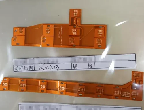
FPC Design: Materials, EDA Tools, and Signal Integrity Guide


Manufacturers create a Flexible Printed Circuit Board (FPC) as a high-performance electronic interconnect component using precision etching processes, with a flexible polymer material (such as polyimide or polyester film) serving as the dielectric layer.
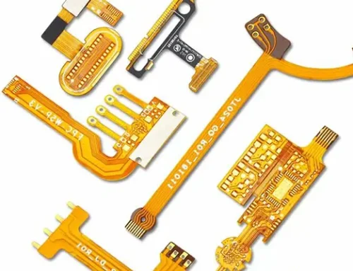
Compared to rigid circuit boards, designers can bend, fold, and twist FPCs, allowing them to adapt to complex three-dimensional layouts.
They offer significant advantages in applications requiring thin and lightweight designs, dynamic bending, and high-density wiring.
FPCs primarily consist of a flexible substrate, conductive copper foil, and a dielectric protective layer.
Manufacturers fabricate them into single-layer, double-layer, or multi-layer circuit structures by transferring circuit patterns, etching, punching, laminating, coating films, and using through-holes to achieve interlayer connectivity.
Their core advantages include:
- ultra-thin and ultra-light designs with thicknesses less than 0.1 mm;
- the ability to withstand tens of thousands of repeated bends;
- and excellent vibration and shock resistance achieved through highly integrated flexible connections.
These characteristics make them widely applicable in consumer electronics (such as foldable phones, smartwatches, and action cameras), automotive electronics (such as in-vehicle sensors, lighting control, and instrument displays), medical devices (such as endoscopes, ultrasound probes, and cochlear implants), as well as aerospace and industrial automation (such as satellites, drones, and high-speed rail control systems).
With advancements in material innovation (such as high-thermal-conductivity substrates) and process upgrades (such as laser processing and 3D printing), FPCs are driving the development of emerging fields such as flexible electronics, wearable devices, and new energy vehicles, serving as a crucial technological foundation for the miniaturization and functional integration of modern electronic products.
This article will address the complexity and unique characteristics of FPC design, providing practical guidance for FPC EDA design through case studies and technical discussions.
Key Technologies and Practices in FPC Circuit Design
This chapter will analyze the flexible printed circuit board design process, exploring aspects such as EDA tool selection, analysis of typical design cases, FPC material and structural design, impedance control, and signal integrity.
Selection of EDA Tools
Electronic Design Automation (EDA) refers to the use of advanced computer software to assist in the design and manufacturing of electronic products.
Designers now widely use EDA software in various fields, including electronic circuit design and simulation, as well as chip design and verification.
Taking FPC design as an example, designers use Altium Designer (formerly known as Protel) as a mainstream EDA design software.
As a leading international EDA tool, Altium Designer offers comprehensive and professional capabilities, supporting complex design requirements such as multilayer boards, high-speed signal routing, rigid-flex board design, and 3D modeling and simulation (e.g., signal integrity analysis and electromagnetic compatibility analysis).
Its interactive routing engine and constraint management features perform exceptionally well in complex projects.
Additionally, Altium Designer supports multi-team collaborative design, making it suitable for large enterprises or highly complex projects.
While Altium Designer excels in functional depth and professionalism, Lichuang EDA focuses on low cost, ease of use, and ecosystem integration as its core competitive advantages.
The choice between the two should be based on a comprehensive evaluation of project requirements, budget, and the team’s technical capabilities.
Analysis of Typical Design Cases
This section analyzes common scenarios encountered in the flexible printed circuit board (FPC) design process, such as importing CAD drawings into Altium Designer, drawing special packages, and copper plating for FPC boards.
› Importing AutoCAD Drawings
In the Altium Designer project development process, division of labor and collaboration are essential.
EDA engineers and the project team’s mechanical and structural engineers typically determine the physical form of an FPC board through collaborative design efforts.
In most cases, based on the circuit layout and mechanical structure of the product, the layout size and dimensions of the FPC board are first drawn in computer-aided design (CAD) software such as AutoCAD.
If designers have already created the FPC board’s outline and layout dimensions in CAD software, they can directly import them into EDA design software.
Taking Altium Designer as an example, the import steps are as follows.
1) In AutoCAD, designers should position the content containing the FPC board outline and dimensions close to the upper-right corner of the drawing origin. If you are unsure of the origin’s location, copy the content to a new drawing.
2) In Altium Designer, create a new PCB drawing to import the FPC board outline and set the origin. We recommend placing a pad at the origin to facilitate quick scaling and positioning.
3) Go to “File” → “Import” → “DXF/DWG” to load the corresponding AutoCAD drawing into Altium Designer.
In the “Import from AutoCAD” dialog box, set the ‘Scale’ parameter to mm, the “Default Line Width” parameter to 0.2 mm, and under “Layer Mapping,” set the “Source Layer Name” parameter (where the value is 0) to “Keep-Out Layer” as shown in Figure 1.
4) Adjust or hide layers as needed, delete redundant content, and retain only the Keep-Out Layer as the board outline.
5) Select all Keep-Out board outline lines, then use “Design” → “Board Shape” → “Define by Selected Objects” to define the board outline display area, facilitating subsequent design work.

Figure 1: Layer mapping parameter settings
› Drawing Custom-Shaped Pad Packages
The Altium Designer package library primarily provides standard circular, elliptical, and rectangular pad packages.
However, FPC designs often require the creation of special pad packages, namely custom-shaped pads.
Designers can create these custom-shaped pads directly within the package library, or they can first draw the required shape or block on the PCB layout and then paste it into the corresponding layer of the pad package.
Step-by-Step Creation of Custom Pad Packages
Next, we will use the custom-shaped pad shown in Figure 2 (indicated by the arrow) to illustrate the steps for creating the package.
1) Pad Outline:
On the Top Layer of the PCB layout, draw the outline that will later serve as the copper area for the irregular-shaped pad.
2) Clearance Setup
Set the global clearance in the PCB rules to 0.75 mm. Designers can adjust the specific value based on design requirements.
In this example, as shown in Figure 3, designers set the solder mask window back 0.75 mm relative to the copper area.
3) Inset Boundary
Select the outline drawn in Step 1, then use the “Tools” → “Trace Selection” function to generate “Inset” and ‘Extend’ lines.
Here, retain the “Inset” line as the boundary for the non-circular pad’s solder mask opening (Top Solder) and stencil aperture (Top Paste).
Note: In this example, the irregular-shaped pad solder mask openings and stencil apertures are the same size.
4) Slot Creation
Draw the slot borders at the corresponding positions on the top, left, and right sides, and use “Tools” → “Convert” to convert them into cutting slots.
5) Fill Generation
On the PCB Top Layer, select the borders drawn in Steps 1 and 3, respectively, and use “Tools” → ‘Convert’ → “Create Area from Selected Elements” to generate Fill Block 1 for the custom pad copper fill, and Fill Block 2 for the custom pad solder mask openings and stencil openings.
6) Library Import
Create a new package in the PCBLib package library. At the origin, paste Fill Block 1 (created in Step 5) onto the package’s Top Layer; paste Fill Block 2 onto the package’s Top Solder mask layer and Top Paste layer.
7) Pad Placement
Finally, be sure to place a top-layer surface-mount pad labeled “1” at the origin to serve as the electrical connection point for the irregular-shaped pad package.
The final result of the irregular-shaped pad package is shown in Figure 3.

Figure 2: Actual product of irregularly shaped solder pads

Figure 3: Irregularly shaped pad package
› Considerations for Copper Padding on FPC Boards
Copper padding is a critical aspect of PCB design. It involves covering the blank, untraced areas of the PCB with a copper layer.
Its benefits include reducing ground impedance, enhancing noise immunity, minimizing voltage drops, improving power supply efficiency, and connecting to the ground to reduce loop area.
The following points should be noted when performing copper plating on FPCs.
1) Generally, high-frequency circuits have higher requirements for noise immunity, so a grid-pattern copper plating is often used; low-frequency circuits or circuits with high current typically use large-area copper plating.
2) FPCs are prone to distortion and tearing at bends; it is recommended to add tear-resistant copper strips along the edges of the FPC board or to use a grid-pattern copper plating at the bends.
3) To ensure signal transmission quality, copper patterns should ideally be laid out at a 45-degree angle, with both line width and spacing set to 0.2 mm.
4) For large-area copper patterns on FPCs, if air is not completely evacuated during the coverlay lamination process, it may react with moisture, leading to surface oxidation.
It is recommended to address this issue using gold plating or OSP (Organic Solderable Protective) processes.
5) Since the core material of FPCs is relatively thin, it is recommended to add copper plating when surface-mount components are present on both the top and bottom layers.
Use cross-connection (Relief Connect) pads for the copper plating, and stagger the layout of the surface-mount pads on the top and bottom sides to avoid stress concentration and improve soldering and signal integrity.
› 3D Model Loading and 3D Preview
Altium Designer provides a 3D preview feature for circuit boards. Figure 4 shows a 3D preview of an FPC board.

Figure 4. 3D preview of the FPC board.
The 3D preview allows for an intuitive assessment of potential interference or obstruction between components on the designed FPC or with other mechanical parts.
It also enables early detection of manufacturing risks, such as whether the trace layout is reasonable or if vias are too close to pads or board edges, and identifies issues such as via plating or incorrectly configured pad cutouts.
To enable a 3D preview of a PCB, all components on the board must have 3D package models.
Altium Designer provides 3D models for the most commonly used components.

Figure 5 shows that the 3D model and the package pads are not aligned.
For newer components or connectors, you can use custom models (be sure to accurately verify the component’s actual dimensions to avoid assembly errors), update the model library, or contact the manufacturer directly to obtain the required STEP-format file (3D model file), which can then be loaded into the corresponding package’s model library.
When adding a model for the first time, the 3D model and package pads may not align, as shown in Figure 5. This can be corrected by rotating and translating the model in 3D to achieve the correct alignment shown in Figure 6.

Figure 6 shows the 3D model, and the package pads are now connected.
› Special Handling of the Silkscreen Layer
To address DRC (Design Rule Check) errors caused by the silkscreen, you can adjust the silkscreen position as needed or temporarily disable the silkscreen clearance DRC check.
When the FPC board has few components and sufficient space, the silkscreen can be directly incorporated as a top layer or bottom layer, achieving the silkscreen effect through the copper foil.
This approach not only improves the visibility and durability of the silkscreen but also reduces manufacturing costs (by eliminating the process step of printing the silkscreen layer).
To ensure a safe distance between the copper fill and the silkscreen around the traces, first draw a border around the silkscreen on the Keep-Out layer, then designate it as a copper-free region (Region), and finally delete the border on the Keep-Out layer. The result is shown in Figure 7.

Figure 7 Copper screen printing copper layer
› Inserting Tables into PCB Layouts
Similar to silkscreen processing, if you want to enhance the durability of the table’s silkscreen, you can also incorporate the table directly as a top layer or bottom layer, provided there is sufficient space on the FPC board.
To do this, use “Place” → “Objects from File” to insert the table into the PCB; the table will then exist as a Region block.
If the text size in the PCB table appears too large, you can first reduce the font size to a suitable level in the table file and then reinsert it.
To adjust the thickness of the PCB table, you can change the table size by right-clicking → “Union” → “Adjust Union Size.” If the result is unsatisfactory, you can first “Ungroup the object union” (retaining only the text) and then redraw the table border lines. The result is shown in Figure 8.

Figure 8. Drawing of copper sheet table
It should be noted that a Keep-Out zone for copper pour does not need to be set around the perimeter of the table, as the table itself has a border. If copper pour is required around the table, ensure a safe distance is maintained between the pour and the table in the safety margin settings to prevent DRC (Design Rule Check) errors.
FPC Materials and Structural Design
The copper foils used on FPC boards are primarily of two types: electrolytic copper foil and rolled copper foil.
Manufacturers produce electrolytic copper foil through an electrochemical deposition process, while they produce rolled copper foil through a physical rolling process. The differences in these manufacturing processes result in distinct physical properties.
› Performance Differences and Application Selection
Overall, manufacturers offer electrolytic copper foil with low cost and high adhesion, making it suitable for general-purpose circuits; they prefer rolled copper foil for high-end electronic devices due to its high flexibility and high-frequency performance.
When selecting materials, it is necessary to balance cost, signal requirements, and mechanical environments.
For example, designers must use rolled copper foil for FPCs in dynamic bending scenarios, while they can select electrolytic copper foil for general consumer electronics to reduce costs.
FPCs are classified into single-sided, double-sided, and multilayer boards based on the number of layers.
Designers typically determine the number of layers during the design phase, so they can select the appropriate layer count directly according to design requirements.
Calculating the thickness of an FPC board requires a comprehensive consideration of material type, laminate structure, and application requirements.
The sum of the substrate thickness (e.g., polyimide or PI), copper foil thickness (electrolytic or rolled copper foil), cover layer thickness (cover film or ink), and reinforcement material thickness (e.g., FR4, steel foil, or PI reinforcement) determines the total thickness.
› FPC Total Thickness Calculation Formula
The specific formula for calculating the total thickness is as follows:
Total thickness equals the sum of base material thickness, twice the copper foil thickness (for double-sided boards), twice the cover layer thickness (for double-sided boards), and reinforcement material thickness (note: “double-sided” refers to the top and bottom copper foil and cover layers; for multilayer boards, designers must add the thicknesses of the corresponding layers).
Engineers must also confirm actual material thicknesses with the manufacturer (as tolerances may vary) and consider factors such as FR4 prepreg resin flow and copper residue rates.
Impedance Control and Signal Integrity
Impedance calculations for FPC boards require a comprehensive consideration of material properties, laminate structure, and trace parameters. Common impedance types include single-ended line impedance (characteristic impedance) and differential impedance, with their respective formulas shown below.
1) Single-ended line impedance:
The single-ended line impedance formula applies to microstrip structures and uses an empirical formula, as shown in Formula (1).
Formula 1
Where: εr represents the dielectric constant of the substrate, H represents the dielectric thickness between the signal line and the reference plane, W represents the trace width, and T represents the copper foil thickness.
2) Differential Impedance:
The differential impedance formula is approximate, as shown in Formula (2).
Formula 2
Where: S represents the spacing between the differential pairs, and H represents the dielectric thickness.
Suppliers provide the dielectric constant and loss factor of specific materials in datasheets, or engineers determine them through actual measurements.
The relationship between differential impedance (Zdiff) and single-ended impedance (Z0) primarily depends on the coupling conditions.
Without coupling, Zdiff equals twice Z0; with coupling, designers must consider odd-mode impedance (Zodd).
Applicable scenarios involve factors such as high-speed signals, routing density, and loss control. Table 1 shows the differential impedance calculations and design considerations for different application scenarios.
| Scenario | Differential Impedance Formula | Design Guidelines | Typical Applications |
|---|---|---|---|
| Uncoupled Differential Pair | ( Zdiff = 2Z0 ) | Control spacing ≥ 3× trace width | Low-frequency, low-density routing scenarios |
| Tightly Coupled Differential Pair | ( Zdiff = 2Zodd ) | Optimize trace width/spacing, validate with simulation | High-speed interfaces (USB/HDMI), RF front-end |
| Loosely Coupled Differential Pair | Formula (2) | Balance insertion loss and routing space | Long-distance transmission (backplane interconnects, Ethernet) |
Table 1: Differential Impedance Calculations and Design Considerations for Various Scenarios
In addition to using formulas, engineers can also use specialized impedance calculation tools to perform impedance calculations.
PolarSi9000 supports a variety of transmission line models and enables impedance calculations for high-frequency and complex structures.
FPC board impedance calculations must integrate material properties, layer stack-ups, and manufacturing capabilities, utilizing a combination of formula-based calculations and simulation tools for collaborative optimization.
For complex scenarios (such as high-frequency and high-density interconnects), designers should work closely with manufacturers and use measured data to iterate the design, ensuring signal integrity.
Conclusion
Looking ahead, FPC technology will continue to push the boundaries of thinness, lightness, and reliability, driving innovation in fields such as consumer electronics, automotive electronics, and medical implantable devices.
With the growing demand for high-frequency and high-speed applications in 5G and 6G, FPC will also integrate new materials—such as ultra-thin PI and nano-copper foil—and advanced processes like laser 3D printing to achieve higher integration and improved bend life.
AI-driven design will accelerate development cycles, and the concept of green manufacturing using biodegradable substrates has also become a trend.
FPC is evolving from “flexible connectivity” to “intelligent flexible systems,” reshaping the form factor of next-generation electronic products.