How to Prevent FPCB Pad Cracking: Bump Design, Material Selection & Stamping Process Guide

Flexible printed circuit boards (FPCBs) are core components used to achieve flexible connections in electronic devices.
To ensure better contact between certain specialized devices and other components, the bump process is employed on the connection pads of FPCBs.
For example, this technology is used in the SIM card slots of point-of-sale (POS) systems, printer cartridges, and other devices.
The reliability of the bumps directly affects product performance and service life, and bump cracking is a common failure mode in FPCBs during manufacturing, assembly, or use.
This paper provides an in-depth exploration of the causes of bump cracking from the perspectives of engineering design, material selection, and stamping methods.
Bump Design
Introduction to Bumps
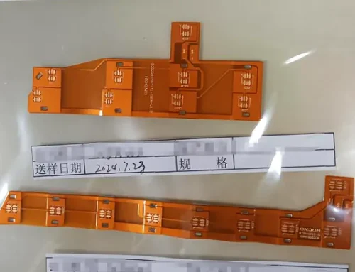
FPCB bump technology refers to the formation of metal bumps with specific heights and shapes at specific locations on an FPCB, as shown in Figure 1.

Figure 1: Actual view of the connection pad bumps on an FPCB
These protrusions play a critical role in electronic devices by providing electrical connections and mechanical fastening.
Typically, the center of the connection pad is raised through stamping or localized plating to increase its thickness; this paper focuses primarily on the application of stamping methods.
Design Requirements for Pad Connectors
To prevent tearing or collapse of the copper foil during the stamping process, the relationship between the pad height (H), substrate thickness (T), and pad diameter (D) is shown in Figure 2. The specific requirements are as follows:
(1) When the pad height H is greater than 0.5 times the substrate thickness T, the pad diameter must satisfy D ≥ 1.8H. For example, if H = 0.30 mm, then D ≥ 0.54 mm.
(2) When the pad height H = T, the diameter must satisfy D ≥ 2.5H. For example, if T = 0.10 mm, then D ≥ 0.25 mm.

Figure 2: Bump connectors on an FPCB
Experiment 1: Effect of Connection Pad Design on Bump Cracking
Connection Pad Dimension Specifications
There are two categories of pad sizing constraints: one is defined by the copper foil, known as a copper-defined pad (CD Pad) or non-solder-mask-defined pad (NSMDP), commonly referred to as an “unmasked pad” in FPCB design, as shown in Figure 3(a).
The other type of connection pad is defined by the solder mask pattern, known as a solder mask defined pad (SMDP), commonly referred to as a “masked pad” design in FPCB, as shown in Figure 3(b).
Since FPCBs use a cover film instead of a solder mask, this type of connection pad can be further classified into cover film defined pads and non-cover film defined pads.

Figure 3: Dimensions of the Coupling Plate
Bump Pad Design
Single-Sided Bump Pad Design
Single-sided pad-on-pad designs must be configured as “press-to-pad” types, utilizing a specialized structural design for surface-mount devices (SMD).
This design ensures that the cover film fully presses against the area surrounding the pad, creating a secure bond.
The primary objective is to prevent cracking or damage to the polyimide (PI) substrate during the pad-forming process, as shown in Figure 4.
The PI thickness of FPCB substrates is typically only 25 μm. If the area around the connection pad is not effectively bonded by the cover film, the PI material in that region lacks support.
As a result, it becomes exceptionally fragile. It is highly susceptible to cracking when subjected to mechanical stresses such as stamping, which in turn affects the product’s reliability and service life.

Figure 4: Single-sided FPCB connector board design
Design of Double-Sided Pad Connectors
The pad surface of the double-sided connector features a circular cutout, while the recessed surface is designed as a square, as shown in Figure 5.
It is important to note that the dimensions of the two connector surfaces and their cutouts must differ; if designed with identical dimensions, the connector may detach.
This conclusion has been verified by JaliChuang FPCB.

Figure 5: Design of a Double-Sided FPCB Connector Plate
Pressure PAD Test Protocol and Results
To verify the impact of different pressure PAD designs on pad cracking, conducted an in-depth study on pad surfaces using both pressure PAD and non-pressure PAD designs.
The tests utilized 0.11 mm thick boards made of 12 μm adhesive-free electrolytic copper, with 16 pieces of each design, all stamped using the same set of steel dies.
The results showed that 3 pads (15%) cracked in the pressed PAD design, while 17 pads (85%) cracked in the unpressed PAD design. The test samples are shown in Figure 6.
The experimental results show that cracks appeared in both the pressure-applied PAD and the non-pressure-applied PAD.
However, the pressure-applied PAD design exhibited significantly fewer cracks than the non-pressure-applied PAD, and the severity of the cracks was relatively milder.

Figure 6: Effect of Pressing the PAD vs. Not Pressing the PAD on the Contact Points
Experiment 2: The Effect of Electrolytic Copper and Rolled Copper on Protrusions
Introduction to Electrolytic Copper and Rolled Copper
This method has low production costs and a mature process, making it suitable for large-scale mass production.
Produce rolled-annealed (RA) copper by subjecting high-purity copper ingots to repeated hot rolling, cold rolling, and annealing processes.
It features a horizontal lamellar grain structure and excellent ductility; however, the process is complex, requires high equipment precision, and is significantly more expensive than electrolytic copper.
Test Protocol and Results for Copper Foil Types
The test used 0.11 mm thick boards made of 12 μm adhesive-free electrolytic copper and rolled copper.
All test samples featured a pressed PAD design, with 16 pieces per group, and used the same set of steel dies for stamping.
To verify the performance of pressed PADs made from electrolytic copper and rolled copper, tested 20 raised points for each material.
The results showed that 4 raised points (20%) in the electrolytic copper sample fractured, while none (0%) of the raised points in the rolled copper sample fractured; all rolled copper samples passed the test.
Experiment 3: The Effect of Different Stamping Dies on Protrusions
Introduction to Stamping Dies
Identify two main types of dies for stamping protrusions: bakelite dies and steel dies, as shown in Figure 7.
")
Figure 7: Bakelite jig and steel mold (actual items)
Bakelite molds are inexpensive to manufacture and are suitable for low-cost or single-use applications. Steel molds are more expensive to produce.
However, they offer better cost efficiency in mass production due to the ability to spread costs over a larger volume.
See Table 1 for a detailed comparison of their specific characteristics.
| Comparison Aspect | PCB Fixture (Phenolic / FR-4 Type) | Steel Mold |
|---|---|---|
| Main Material | Phenolic resin base with wood powder filler, compression molded | Steel (e.g., carbon steel, tool steel) |
| Hardness | Lower hardness (Rockwell ~70–90), moderate wear resistance | Higher hardness (Rockwell ~85–98+), strong wear resistance |
| Heat Resistance | Withstands ~120–150°C; may deform or soften under prolonged heat | Excellent heat resistance (some steels withstand >300°C) |
| Electrical Property | Good insulation, suitable for electronics fixtures | Conductive, no insulation |
| Weight | Lightweight, easy to handle and install | Heavy, typically used with stamping presses |
Table 1: Differences Between PCB Fixtures and Steel Molds
Test Protocol and Results for Molds of Different Materials
The test used 0.11mm thick, 12 μm adhesive-free rolled copper sheets.
All test samples featured a PAD design, with 16 pieces per group, and used both bakelite molds and steel molds for stamping.
During the validation process, used both bakelite molds and steel molds to stamp 20 copper-clad laminate PAD bumps.
The results showed that 4 bumps (20%) fractured in the Bakelite molds, and the bump surfaces were sharp and rough.
Conclusion
This experiment investigated the effects of engineering design, copper foil type, and stamping dies on the formation of cracks in FPCB connection pad bumps. The results are as follows:
(1) Recommend rolled copper, as electrolytic copper poses a certain risk of bump cracking.
(2) For sample production, consider using bakelite jigs; however, for mass production, recommend steel molds.
This experiment has preliminarily validated the key control points for FPCB pad connection plates.
However, numerous factors remain unaccounted for. These include differences between single-sided and double-sided boards.
They also include the impact of copper thickness on pad cracking. Additionally, distinctions between adhesive-free and adhesive-coated substrates remain unaddressed.
We have not yet considered variations in supplier materials. We look forward to further discussion and in-depth study with process engineers within the industry.