Rigid-Flex PCB Manufacturing: Process Optimization for Outer-Layer Flexible Structures
Rigid-flex printed circuit boards (R-FPCBs) combine the advantages of both rigid and flexible boards. As printed circuit boards (PCBs) continue to evolve toward being lighter, thinner, and smaller, the demand for these products is growing steadily.
While the design of R-FPCBs offers significant convenience, it also presents greater challenges than the manufacturing processes for conventional rigid PCBs (rigid boards).
There are various laminate structures for R-FPCBs; a common configuration features a symmetrical structure where the flexible portion is the middle layer.
This paper introduces a structural configuration where the flexible portion is located on the outer layer.
It analyzes the advantages and disadvantages of the manufacturing process for this type of R-FPCB.
It also optimizes the process flow and methods to effectively resolve technical challenges encountered during production.
Basic Product Information
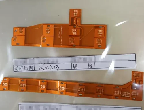
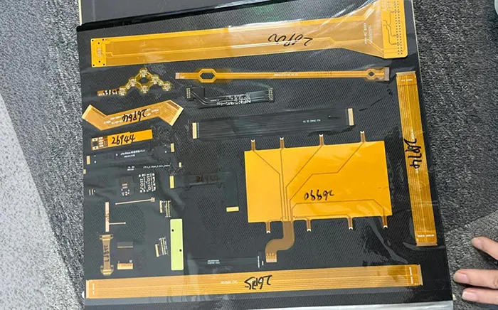
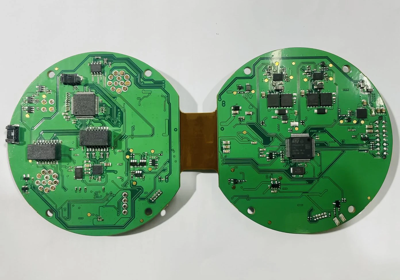
Basic product information is provided in Table 1, and the finished product is shown in Figure 1.
| Item | Specification |
|---|---|
| Layer Count (L) | 8 layers (including 2 flexible layers) |
| Finished Board Thickness (mm) | 1.60 ± 10% |
| Substrate Materials | FR-4, Polyimide (PI), Prepreg (PP), Coverlay (CVL) |
| Panel Size (mm) | 457 × 610 |
| Finished Product Size (mm) | 294.00 × 213.56 |
| Inner Layer Copper Thickness (μm) | 18 |
| Outer Layer Copper Thickness (μm) | Min. 38.4 |
| Minimum Drill Hole Diameter (mm) | 0.20 |
| Flexible Area Thickness (mm) | 0.22 ± 0.05 |
| Surface Finish | Electroless Gold (Chemical Gold) |
Table 1: Basic Product Information

Figure 1 R FPCB Product
Manufacturing Process for Rigid-Flex Printed Circuit Boards with a Flexible Layer on the Outer Layer
Conventional Process Flow
The laminated structure of a rigid-flex printed circuit board with a flexible layer on the outer layer is shown in Figure 2.
The conventional manufacturing process flow is shown in Figure 3, where AOI stands for Automated Optical Inspection.

Figure 2 Laminated stack structure

Figure 3: Conventional manufacturing process for R FPCBs with a flexible substrate on the outer layer
Issues in the Manufacturing Process
After lamination, indentations appear in the rigid-flex junction area, causing the outer laminate to adhere poorly.
This leads to defects in the outer circuit layer, resulting in low yield rates, difficulties in quality control, and increased costs.
Two Improved Process Methods
Improved Method 1
Stackup Adjustment
The stackup is adjusted to a two-step lamination process. In the first step, conventional flowable PP is used to laminate the rigid board sections first; in the second step, the flexible board is laminated with the semi-finished rigid board sections.
The non-flowable PP corresponding to the flexible area is treated with a window cutout, and the cutout area is filled with a spacer to reduce the height difference in the flexible region.
During lamination, a 0.5–1.0 mm thick FR-4 pressure-supporting sheet is placed on the flexible board to prevent indentations or depressions in the flexible area after lamination.
This avoids difficulties in subsequent manufacturing processes and prevents quality issues. The stack-up is shown in Figure 4.
")
Figure 4 Laminated structure of Method 1 (modified)
Process Flow
The process flow for Method 1, as modified, is shown in Figure 5.
")
Figure 5 Process flow for Method 1 (improved)
Final Results
After lamination, the flexible area remained intact with no signs of indentation, thereby resolving the issues of lamination indentation and defects in the outer layer circuits.
Improved Method 2
Stack-up Adjustment
The stack-up is adjusted to a single lamination. For the non-flowing PP and FR-4 materials corresponding to the flexible zone, a windowed design is implemented.
The windowed areas are filled with shims to reduce the height difference in the flexible zone.
When pre-stacking the laminate, add FR-4 pressure-compensating sheets with a thickness of 0.5–1.0 mm to both the top and bottom surfaces.
This resolves the issue of indentations in the flexible zone after lamination, thereby preventing manufacturing difficulties and quality defects in subsequent processes.
The stack-up is shown in Figure 6.

Figure 6 Laminated structure of the improved Method 2
Process Flow
The process flow for Improvement Method 2 is identical to that shown in Figure 3 of Section 2.1, with the sole difference being the lamination stackup.
Final Results
After lamination, the flexible area remained intact with no indentations or dents, thereby resolving the issues of lamination indentation and defects in the outer layer circuits.
Comparison of Advantages and Disadvantages
Table 2 presents a comparison of the advantages and disadvantages of different manufacturing processes for R-FPCBs with a flexible layer on the outer surface.
| No. | Manufacturing Process | Advantages | Disadvantages |
|---|---|---|---|
| 1 | Conventional Lamination Process | Short production cycle | Low yield, difficult quality control |
| 2 | Laser Blind Via Process | High yield, easy quality control | Long production cycle, high cost |
| 3 | Lamination Process with Added FR-4 Reinforcement | Short production cycle, high yield, easy quality control | Slightly higher cost |
Table 2: Comparison of Advantages and Disadvantages of Different Manufacturing Processes
Conclusion
This paper examines two manufacturing processes for RF-FPCBs with flexible panels on the outer layers.
It conducts a comparative analysis of methods such as laser blind via technology and the addition of FR-4 backing sheets during lamination, reaching the following conclusions:
(1) Process Optimization Strategies to Prevent Flexible Area Indentation
When using the PP windowing technique adjacent to the flexible area and incorporating spacer fillers during fabrication, there is a risk of indentation in the flexible area during lamination.
Compared to the laser blind via method, this approach shortens the production cycle and reduces production costs.
(2) Validation of Optimized Processes
Validation of the two improved process methods confirmed that both can produce qualified R-FPCBs for the outer layer of flexible boards.
Additionally, they reduce the risk of indentation in the flexible zone during lamination and prevent open circuits or short circuits during the fabrication of the outer layer circuits.
(3) Validated Manufacturing Process
The team successfully validated the manufacturing process for R-FPCBs with a flexible board on the outer layer.
This process offers the advantages of a simple workflow, ease of operation, high yield rates, easy quality control, and diverse implementation methods.