Inner-Layer Pad Protection Methods for FPC: Materials, Processes, and Comparative Analysis

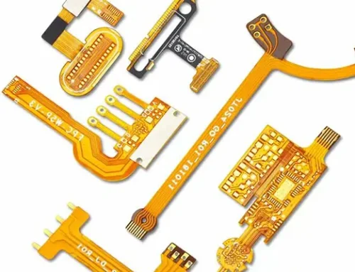
With the rapid advancement of electronic technology, standard single- and double-sided flexible circuit boards can no longer meet customer needs, leading to a growing demand for highly integrated, multilayer flexible boards and rigid-flex boards.
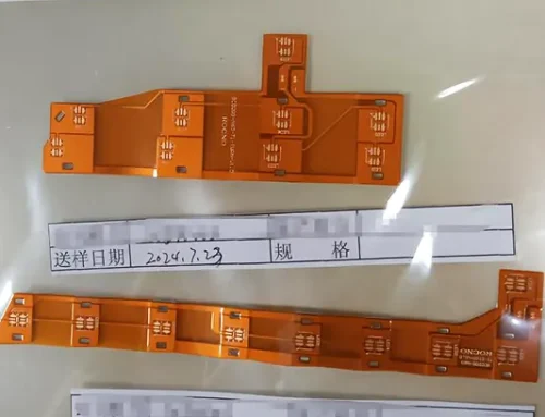
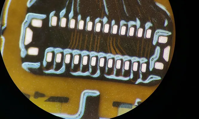
When designing multilayer flexible boards, inner-layer pads often need to remain exposed.
Therefore, during fabrication, the copper in these areas must be protected to prevent it from being etched away by the chemical solution during the formation of outer-layer patterns, which would render the board unusable.
Typically, inner-layer pads have irregular shapes and are randomly distributed, which increases the difficulty of effectively protecting them.
This paper conducts a comparative analysis of the advantages and disadvantages of four experimental approaches based on material properties, manufacturing costs, efficiency, and reliability.
Four Methods for Protecting Exposed Inner-Layer Pads
High-Temperature Adhesive Tape Method
1. Method Overview
Cover the inner-layer pads that require protection with strips of high-temperature adhesive tape. After the outer-layer traces have been completed, manually peel off the tape (Figure 1).

Figure 1: High-temperature-resistant tape
As shown in Figure 2, the area within the box is the adhesive-free zone, where the high-temperature-resistant tape is applied; the area outside the box is the adhesive zone (epoxy thermosetting adhesive).
The width of the high-temperature-resistant tape can be selected according to requirements, with different width specifications available for purchase to accommodate PCB manufacturers’ production needs.
The high-temperature-resistant tape strip is applied to the adhesive-free area, and both its length and width must be slightly smaller than the length and width of the adhesive-free window (the optimal distance between the tape edge and the AD adhesive/PP sheet is 1 mm, with a minimum of 0. mm).

Figure 2: High-temperature-resistant tape bonding area
2. Process Flow
The process flow is shown in Figure 3.

Figure 3: Process Flow
3. Properties of High-Temperature Adhesive Tape
High-temperature resistant tape [1] primarily consists of two main components: the substrate and the adhesive. Substrate materials include polyimide (PI), PTFE-coated glass fiber cloth, and polyester (PET), while adhesives include silicone, polyacrylate, and rubber (natural rubber, EPDM, and neoprene).
By combining different substrates with adhesives, high-temperature-resistant tapes can be produced to meet various requirements.
Among these, tapes with a polyimide film substrate and silicone adhesive offer the best high-temperature resistance, featuring excellent insulation, puncture resistance, and acid/alkali resistance.
They can withstand temperatures of 300°C for 10 minutes and can be used continuously at 100°C.
However, after removing the high-temperature tape, adhesive residue often remains on the solder pads or finger areas, posing significant quality risks for subsequent processes (Figure 4).

Figure 4
4. Analysis of the Advantages and Disadvantages of High-Temperature Adhesive Tape (Table 1)
The analysis of the advantages and disadvantages of high-temperature adhesive tape is shown in Table 1.
| Category | Description |
|---|---|
| Advantages | 1. Low cost, easy to operate; can be directly applied according to the marking lines on the board surface. |
| 2. Resistant to high temperature and high pressure (short-term); resistant to acids and alkalis, wear-resistant, crack-resistant, with strong adhesion. | |
| Disadvantages | 1. Cannot achieve precise local coverage for inner-layer pads. |
| 2. After tape removal, residues may remain on pads and finger positions, affecting subsequent product quality. | |
| 3. Low production efficiency; not suitable for mass production and difficult to scale. |
Table 1: Analysis of Advantages and Disadvantages of High-Temperature Adhesive Tape
Anti-etching Ink Printing Process
1. Process Overview
The engineering design is transferred to a photo, which is then used to expose a screen. After printing the anti-etching ink, it is baked to cure.
When fabricating the outer layer of the circuit, the anti-etching ink can be simply rinsed away.
As shown in Figures 5 and 6, the circular and square ground copper pads are tightly covered and protected by black anti-etch ink.

Figure 5: Pre-printing rendering

Figure 6: Rendering of the final result after printing
After screen printing the anti-etch ink, set the oven curing parameters and cure it.
During the subsequent process of fabricating the outer layer patterns, the ink can be easily removed with an alkaline solution, exposing the inner layer pads and achieving the protection of exposed inner layer pads in multilayer boards.
2. Process Flow
The process flow is shown in Figure 7.

Figure 7: Process Flow
3. Performance of Anti-Etching Ink
The performance of the anti-etching ink is shown in Table 2.
| Item | Specification Requirements |
|---|---|
| Ink Color | Black / Yellow (best matched with coverlay color) |
| Conductivity | Non-conductive, insulating |
| Curing Conditions | Oven curing / Room temperature standing |
| Etching Resistance | Good |
| Lamination Resistance | Good |
| Halogen Requirement | Halogen-free |
| Ink Removal Conditions | 5 s – 10 s at 25°C–50°C in 3%–5% NaOH aqueous solution |
| Ink Removal State | Powdery dissolved material |
| Storage Conditions | 20°C – 30°C, protected from light |
Table 2: Performance Specifications of Anti-Etching Ink
4. Analysis of the Advantages and Disadvantages of Anti-Etching Inks
The analysis of the advantages and disadvantages of anti-etching inks is shown in Table 3.
| Category | Description |
|---|---|
| Advantages | 1. High production efficiency; resistant to high temperature and pressure; strong adhesion; good ink removal performance. |
| 2. Regardless of the shape or distribution of inner-layer pads, precise local coverage can be achieved. | |
| Disadvantages | 1. High cost; poor protection effect for slot and hole positions. |
| 2. Residual anti-etching ink may remain (at the coverlay window opening edges). |
Table 3: Analysis of Advantages and Disadvantages of Anti-Etching Ink
Photoresist Film Application Method
1. Method Overview
For engineering design photomasks, after the photoresist film has been applied to the board (Figure 8), the board is exposed to light.
Following development, the pads that need to be protected are covered and protected by the photoresist film; when fabricating the outer layer circuits, the photoresist film can simply be stripped away.
When designing the dry film exposure pattern, ensure that the dimensions of the protective dry film are appropriate, maximizing the coverage area as much as possible (the dry film must extend at least 1 mm beyond the pads, and the AD edges must extend at least 1 mm beyond the dry film, with a minimum of 0. 5mm).
This prevents damage or detachment of inner-layer pads due to insufficient protective dry film coverage.

Figure 8: Rendering of the dry film application
2. Process Flow
The process flow is shown in the figure 9.

Figure 9: Process Flow
3. Analysis of the Advantages and Disadvantages of Photoresist Dry Film (Table 4)
The analysis of the advantages and disadvantages of photoresist dry film is shown in Table 4.
| Category | Description |
|---|---|
| Advantages | 1. High production efficiency: The entire board is laminated with dry film, and then aligned exposure using a photomask is sufficient. |
| Advantages | 2. High coverage precision: Enables precise local coverage of inner-layer pads. |
| Disadvantages | 1. Not resistant to high temperature and high pressure: After undergoing such processes, the dry film tends to become brittle, resulting in poor protection performance. |
| Disadvantages | 2. Difficult film removal: After stripping, dry film residues may remain at the edges of the openings. |
Table 4: Analysis of Advantages and Disadvantages of Photosensitive Dry Film
“Photosensitive Dry Film + Anti-etching Ink” Combination Solution
1. Solution Overview
The “photosensitive dry film + anti-etching ink” combination leverages the strengths of both materials to provide superior protection for inner-layer pads, thereby further enhancing quality.
First, apply the photosensitive dry film, align, expose, and develop (Fig. 10), then print and cure the anti-etch ink (Fig. 11).

Figure 10: Result after developing the dry film

Figure 11 Rendering of dry film + ink
In this process, specific areas receive dual protection.
Additionally, the dry film serves two purposes here:
(1) protecting the inner-layer pads;
(2) Filling the adhesive-free zones to bridge the height difference between inner and outer layers, thereby increasing the bond strength between the inner-layer and outer-layer copper foil and reducing the risk of delamination during plasma etching before PTH processing.
2. Process Flow
The process flow is shown in Figure 12.

Figure 12: Process Flow
3. Analysis of the Advantages and Disadvantages of the Photosensitive Dry Film and Anti-etching Ink Combination
An analysis of the advantages and disadvantages of the photosensitive dry film and anti-etching ink combination, along with a comparison of various solutions, is shown in Tables 5 and 6.
| Category | Description |
|---|---|
| Advantages | 1. The photosensitive dry film can fill adhesive-free delamination areas, enhancing the bonding strength between inner and outer copper layers, and effectively reducing the risk of delamination during electroplating processes; it also protects inner-layer pads. |
| Advantages | 2. The anti-etching ink has strong pressure resistance and can withstand high temperature and high pressure for extended periods, providing excellent protection. |
| Advantages | 3. For special areas, a combination of “dry film + ink” can be used for double protection, achieving better results. |
| Disadvantages | 1. Higher cost and more complex process. |
| Disadvantages | 2. Longer production cycle, leading to extended delivery time. |
Table 5: Analysis of Advantages and Disadvantages of Photosensitive Dry Film + Anti-etching Ink Combination
| Solution | Advantages | Disadvantages |
|---|---|---|
| High-temperature adhesive tape | Low cost | Low efficiency; prone to adhesive residue |
| Anti-etching ink (printed) | High efficiency; good pressure resistance; strong adhesion; resistant to high temperature and high pressure | High cost; poor protection for slot holes |
| Photosensitive dry film | High efficiency; high coverage precision; relatively strong adhesion | Not resistant to high temperature and high pressure; average film removal performance |
| Photosensitive dry film + anti-etching ink | Good protection performance; high product quality; strong reliability | Complex process flow; more processing steps; relatively high cost |
Table 6: Comparison of Various Solutions
Conclusion
A comparison shows that the “high-temperature-resistant tape” method is inefficient and affects the quality of the product itself.
The “etch-resistant ink printing” and “photosensitive dry film application” approaches each have their own advantages and disadvantages, and their suitability depends on the PCB’s specific laminate structure.
Meanwhile, the “photosensitive dry film + etch-resistant ink” approach yields good results but involves a more complex process and a longer production cycle; therefore, for FPC multilayer boards and rigid-flex boards with different structures, it is necessary to evaluate a reasonable and cost-effective solution based on the company’s own manufacturing processes.