
Wire Harness-Like FPCB Manufacturing Process: Design, Winding and Implementation

However, the Wire Harness-Like FPCB Manufacturing Process turns a bundled copper harness into a single flexible circuit. Therefore, it uses local sub-board slitting, FPCB winding, lamination, and an anti-tear structure to fit a 5 mm-wide space. Additionally, the result carries many traces with ±10% impedance accuracy and bends in non-parallel directions.
Application Scenario: Replacing Bundled Harnesses

Figure 1: Traditional wire harness
Meanwhile, traditional wire harnesses bundle copper wires inside plastic insulation. For example, each harness connects to an electrode, and many harnesses often run in tandem. As a result, the bundle takes up a lot of room inside the vehicle. In addition, space layout becomes a real constraint.
As a result, FPCBs change this picture. In practice, they provide a more organized layout and a more compact structure. Next, they also reduce space demand, improve safety, and cut weight. In addition, flex circuits support automated production and assembly. Consequently, for these reasons, FPCBs first replaced harnesses in battery packs, where they raised both safety and energy density.

Figure 2: FPCB connection module structure in a non-single parallel direction
Moreover, demand then spread. In particular, smart connected vehicles and low-altitude aircraft now use these parts too. However, modules for intelligent control and human-machine interaction followed. However, these new uses put fresh demands on flex design, manufacturing, and performance.
Customer Requirements That Shaped the Design
Therefore, the project focused on an FPCB for a smart connected vehicle battery pack. The customer set clear limits:
- The part must fit a compact space, with width distribution held to 5 mm or less.
- The board must carry many conductive and signal traces.
- Impedance accuracy must stay within ±10%.
- The part must bend in non-parallel directions.
That last point matters. The FPCB sits at the interface between horizontally and vertically mounted modules. A standard single-direction bend cannot serve this joint. Therefore, the part needs non-parallel bending performance.
Novel Structural Design in Wire Harness FPCB Design
Good wire harness FPCB design starts from the assembly, not the artwork. The team weighed three factors together.
First, the connected module dimensions rule out a multi-layer FPCB structure. Such a stack would be too stiff and too thick for the joint.
Second, the non-parallel bending requirement must hold across the whole bend zone. Fold lines cross in different directions.
Third, the process should stay simple and cost-effective without losing performance. Complexity adds cost and risk.
From these inputs, the team built a new structural concept: a harness-like layout with local sub-board slitting. Instead of one wide sheet, the panel splits into local sub-boards. Each sub-board carries its own traces. Together, they route signals much like separate harness strands.
Anti-tear geometry supports this layout. Reinforcement at the bend zones keeps the slitted branches from cracking. As a result, the narrow branches hold up during handling and assembly.
FPCB Winding Lamination: Forming the Harness Shape
FPCB winding lamination is the step that gives the part its harness-like body. The flexible layers are wound and bonded around the routed layout. This step sets the final thickness, bend radius, and layer alignment.
Because the branches are narrow, lamination control matters. Even temperature and pressure keep the adhesive flow uniform. Therefore, no voids form near the slit edges. In addition, the winding direction follows the actual bend path of the joint.
The broader PCB Lamination process follows the same base rules. For more background, the Flexible PCB Process Guide covers cutting, plating, etching, and finishing in order.
Key Technology Analysis and Implementation
Local Sub-Panel Processing and Laminate Anti-Tear Technology
During development, single- or double-sided FPCBs were fabricated with extremely thin thicknesses of 0.12 mm ± 0.03 mm.
Laser cutting or die-cutting techniques were employed to directly create “slits” in the central region of the FPCB, forming the sub-panel structures.
Challenges in Sub-Panel Processing
This process presented two major challenges:
First, since the end regions of the FPCB are interconnected as a single unit, when sub-boards in the central laminated area meet at the interface, significant internal stress is generated within the board body.
This stress readily causes tearing at both ends of the slit.
Second, during mass production using die-cutting technology, the retraction of the cutting tool during the die-back process may pull on both ends of the “slit,” similarly leading to board tearing.
Anti-Tear Solutions
To address these issues, the first solution involves adding “anti-tear holes” at both ends of the processed “slot.” Specifically, before creating the “slot,” through-holes with diameters of 0.15–0.50 mm are pre-drilled at both ends of each pattern.
This technique leverages the stress-relieving or stress-buffering effect of the through-holes during lamination to prevent board tearing.
Second, the “slot” was redesigned as a “through-slot.” This involved widening the slot from 0 mm to 0.2–0.8 mm, creating a channel-like structure after processing.
Punching the “through-slot” with a die provides stress buffering during retraction, preventing tearing caused by retraction forces.
Simultaneously, during lamination of sub-boards, the “through-slot” buffers internal stresses at both ends, further preventing panel tearing during the lamination process. The designed tear-resistant holes and punched “through-slot” structure are shown in Figure 3.

Figure 3: Tear resistant hole and through slot structure plate
Advanced Wire Harness-Like FPCB Considerations
For certain advanced wire harness-like flexible circuit boards with higher requirements and more stringent application conditions, merely incorporating tear-resistant holes may still lead to panel tearing during sub-panel stacking or subsequent insertion/soldering operations, as illustrated in Figure 4.

Figure 4: Tear hole indicates a problem with the plate.
Enhanced Tear-Resistant Hole Process
To address the aforementioned issues, this study further developed a new process.
During the fabrication of single- or double-sided FPCBs, tear-resistant holes are formed along with hole rings.
Depending on application requirements, the single-side width of the hole ring is set between 50 and 300 μm.
For double-sided FPCBs, during the plating process, tear-resistant holes are simultaneously plated to form double-sided hole rings.
During subsequent cover film lamination, windows are first cut in the film at the hole ring locations before application, ensuring the rings remain exposed after lamination.
The copper layer of the hole rings provides enhanced strength and toughness, significantly reducing the risk of substrate tearing during lamination. The improved flat structure of the wire-like FPCB is shown in Figure 5.

Figure 5: Improved FPCB planar structure for wire harness
Selection of Winding Materials and Winding Processing Technology
The FPCB formed via the above process comprises multiple sub-boards. These sub-boards can be further laminated to create a localized laminated wire-like structure.
Laminating Materials and Process
Special laminating materials are required during the lamination process. Since the cover film layer of the FPCB itself carries an acrylic adhesive or epoxy resin adhesive layer, acrylic adhesive or epoxy resin adhesive is typically considered for the laminating adhesive.
The process is completed through the steps of “adhesive layer preparation → lamination → localized pressing.”
Screen printing and semi-curing baking techniques are employed to create the liquid adhesive layer, but this process requires numerous auxiliary tools.
Additionally, since the cover film is made of polyimide material with high inertness, it must first undergo plasma treatment to create a rough surface, further enhancing the bond strength between the adhesive layer and the cover film.
This results in process complexities, high costs, and low yield rates.
Process Challenges and Improvements
Since the laminating process involves non-planar layering, localized compression must be applied to the “central region” after stacking.
This necessitates creating specialized compression molds to ensure precise positioning, which increases costs and complicates the workflow.
Regarding processing quality, using acrylic or epoxy adhesives for laminated compression often leads to edge adhesive overflow issues.
Removing overflow using laser ablation not only adds further steps and costs but also carries the risk of incomplete ablation.
Wire Harness-Like Structure Development
Based on the application scenarios and environments provided by the customer, combined with the structural patterns of traditional wire harnesses, an improved wire harness-like flexible circuit board was developed.
After laminating the sub-boards, this circuit board employs tape wrapping to form a wire harness structure in the central region, while the end regions feature flat mating and soldering surfaces.
Several tapes supporting this design were tested and compared with acrylic or epoxy adhesives. The material with optimal performance is shown in Table 2.
| Item | Acetate Cloth Tape | 3M Tape | Insulating Tape | Acrylic Adhesive | Epoxy Resin Adhesive |
|---|---|---|---|---|---|
Main Material | Acetate cloth composite methyl methacrylate adhesive | Polyphenyl methacrylate adhesive | Polyethylene | Acrylic ester, methyl methacrylate copolymers | Epoxy resin |
High-Temperature Resistance / °C | −40 ~ 150 | −40 ~ 120 | 0 ~ 80 | −40 ~ 150 | −50 ~ 150 |
Corrosion Resistance | Resistant to water, oil, acid, alkali, mold, chemical corrosion | Resistant to water, oil, acid, mold | Resistant to water, acid, mold | Resistant to water, oil, acid, alkali, mold, chemical corrosion | Resistant to water, oil, acid, alkali, mold, chemical corrosion |
Adhesion Strength | Approx. 3.0 N / 25 mm | Approx. 5.0 N / 25 mm | Approx. 2.0 N / 25 mm | Approx. 7.5 N / 25 mm | Approx. 7.5 N / 25 mm |
Service Life / a | >15 | >15 | >10 | >15 | >15 |
Relative Cost | Lower | Higher | Lower | Higher | Higher |
Environmental Performance | Excellent | Average | Average | Average | Average |
Application Technology Requirement | Winding type, relatively simple | Winding type, relatively simple | Winding type, relatively simple | Screen printing or coating type, relatively complex | Screen printing or coating type, relatively complex |
Post-Application Reliability | Firm adhesion, not prone to bubbling | Firm adhesion, not prone to bubbling | Moderate adhesion, prone to bubbling in long-term use | Firm adhesion, not prone to bubbling | Firm adhesion, not prone to bubbling |
Table 2: Performance Comparison of Different Materials
Table 2 indicates that acetate cloth tape offers superior overall performance.
Its inherent flexibility and breathability provide excellent bendability, effectively preventing issues like inadequate heat dissipation during FPCB operation.
Wrapping the sub-board with acetate cloth tape requires no additional tools.
Engineers complete processing by following the “stacking → wrapping” sequence, forming a robust adhesive bond and securing fixation in the stacked area. Additionally, acetate cloth meets most FPCB wrapping requirements.
Figure 6 shows the structure after the engineers performed localized stacked wrapping. For applications demanding higher reliability, acrylic or epoxy adhesives remain viable alternatives.

Figure 6: Improved FPCB-like wire harness structure after partial layering and winding
Through comparative validation, engineers recommend using 0.15 mm thick acetate cloth tape during the manufacturing process of this FPCB product.
The tape width should match the length of the wrapping area (i.e., the distance between the guide lines on both sides of the wrapping zone).
Wrapping 2 to 4 turns ensures good adhesion and restraint, guaranteeing the FPCB’s excellent flexibility.
Impedance Stability Technology
Following the aforementioned process flow, engineers produced an improved wire harness-like FPCB with localized layering and flat ends. As required, the product must exhibit an impedance of (100 ± 10) Ω.
During testing and application, engineers evaluated the impedance of the non-stacked, unwound planar FPCB.
Results confirmed the product’s impedance capability. However, stacking caused mutual interference between impedance lines across sub-boards, resulting in unstable impedance values exceeding specifications.
To address these issues, further research proposed the following measures:
(1) First, apply shielding film to the laminated area of the board, then create gaps or through-slots.
Alternatively, after forming the laminated structure in the laminated area, apply a shielding film to the surfaces of each sub-board located below, then complete the local lamination and wrapping process.
Verification shows this method effectively mitigates excessive and unstable impedance values, controlling impedance within the range of (100±5) Ω.
Engineers may use conventional electromagnetic shielding film or conductive adhesive film. Figure 7 shows the planar structure with the locally applied shielding film.

Figure 7: Planar structure of FPCB with partial shielding film attached
(2) Follow the procedure in Method (1), but replace the shielding film with acetate cloth.
Acetate cloth itself lacks shielding properties, but verification shows that applying it enhances separation between layers in the laminated region, thereby reducing signal interference between layers.
Compared to shielding film, acetate cloth is lower in cost and maintains material consistency with the acetate cloth used in subsequent winding processes.
This avoids processing complexities and significant performance variations caused by using multiple materials.
This approach effectively addresses excessive impedance issues, controlling values within the (100±10) Ω range.
(3) Cover both sides of the circuit layer with shielding copper layers.
This solution operates on the same principle as applying shielding film.
The copper layer can be designed as a mesh pattern to enhance the FPCB’s flexibility, with the cross-sectional structure shown in Figure 8.
This approach has been verified to effectively mitigate excessive and unstable impedance values, maintaining them within the range of (100±5) Ω.
However, this approach requires designing the FPCB as a multilayer structure, increasing manufacturing complexity, difficulty, and cost.
It is suitable when the board demands high structural integrity and precise impedance control.
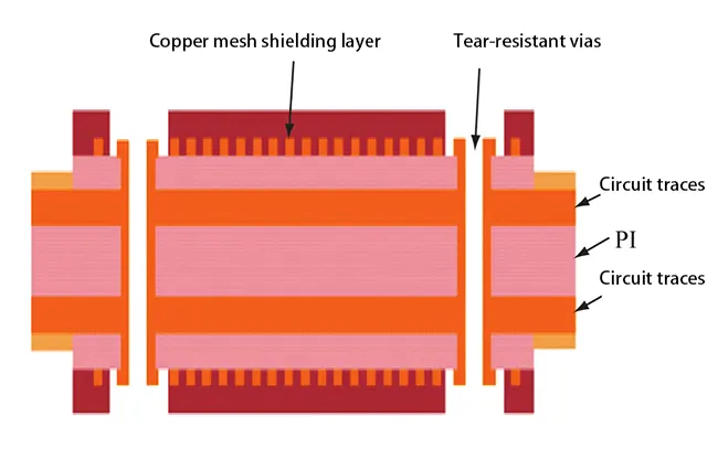
Figure 8: Cross-sectional structure of FPCB with added shielding copper layer design
Product Outcomes
The finished part meets the original targets. It fits the 5 mm width limit and carries the full trace set. Impedance stays within ±10%, and the joint handles non-parallel bending. Compared with the bundled harness it replaces, the FPCB is lighter, thinner and safer. It also supports automated assembly.

The platform now covers related builds, including Double-Sided Flex PCB Manufacturing and High-Reliability Flexible Circuits for High-End Applications.
Conclusions
The Wire Harness-Like FPCB Manufacturing Process combines a harness-like layout with local sub-board slitting, FPCB winding lamination and an anti-tear structure. Each choice follows from the application: narrow space, dense traces, tight impedance and multi-axis bending. Design and process were developed together. As a result, the part replaces a traditional harness without giving up electrical performance. Teams that need a starting point can review the Rigid-Flex PCB Technology notes or the PCB Manufacturing FAQ.
FAQ
What is FPCB winding lamination?
FPCB winding lamination is the manufacturing step that bonds and shapes the flexible layers around a routed, harness-like layout. It fixes final thickness, layer alignment and bend radius. Because the branches are narrow, even temperature and pressure are critical, so no voids form near the slit edges.
How does wire harness FPCB design differ from a standard flex circuit?
A standard flex circuit usually carries one wide, flat body. Wire harness FPCB design splits the panel into local sub-boards, so each branch routes signals like a separate harness strand. It also adds anti-tear geometry and plans for non-parallel bending at the module interface.
Why not use a multi-layer FPCB structure for this part?
The connected module dimensions set the limit. A multi-layer stack would be too thick and too stiff for the joint between horizontally and vertically mounted modules. Therefore, the team chose a simpler structure that keeps manufacturing cost-effective while still meeting the ±10% impedance target.
Related Posts
- Flexible PCB Process Guide — Related article
- Manufacturing Process of Semi-Rigid Flex PCB — Related article
- Multi-layer FPC Manufacturing Process: Cutting to Testing — Related article
- PCB Lamination Process | Rigid & Flexible PCB Manufacturing Guide — Related article
- Rigid Flex PCB Manufacturing: A Process Overview – GekunFlex — Related article