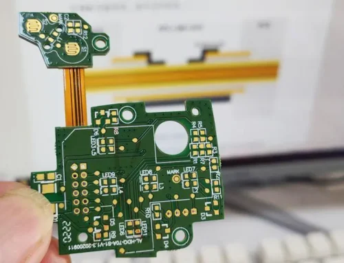
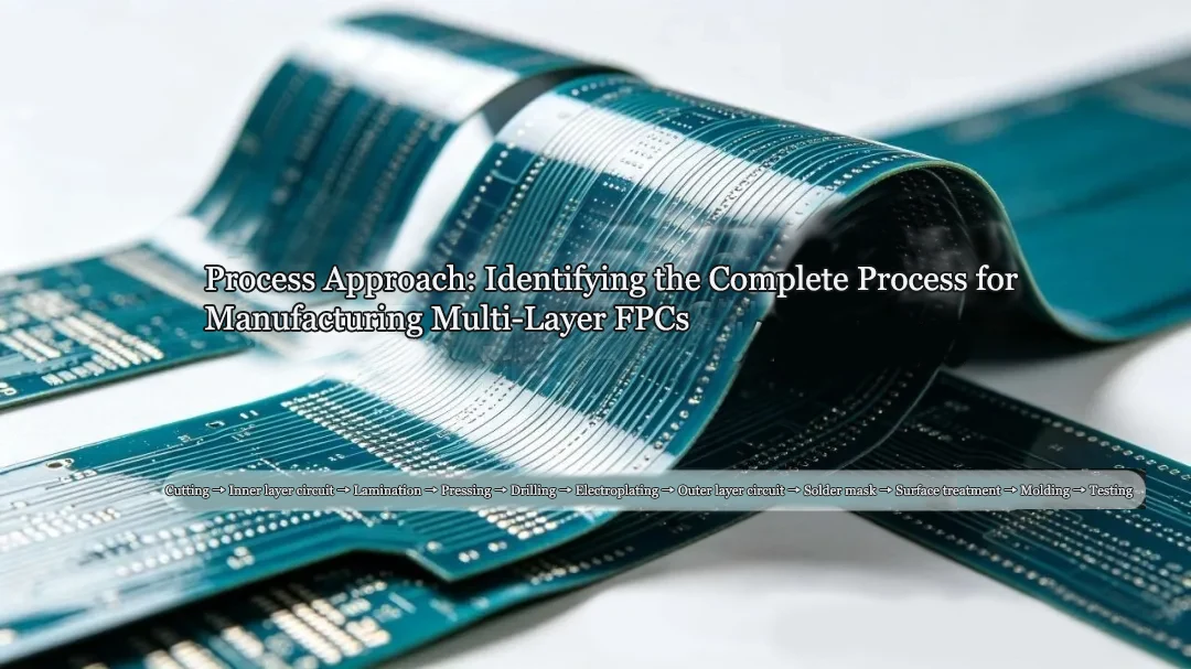
Multi-Layer FPC Manufacturing Process: Complete Step-by-Step Guide from Cutting to Testing
Imagine you are a brand-new FPC. Starting as a roll of golden copper foil, you are about to embark on a long journey through the GenkunFlex Technology workshop.
How long is this journey? At a minimum, it involves a dozen or so processes; at most, over twenty. Each process is a distinct “step.” Every step has an input (what you receive), an activity (what is done to you), and an output (what you become).
If you don’t know where you’re going, which stations you’ll pass through, or what you’re supposed to look like at each stop—you’re likely to get lost, damaged, or even scrapped along the way.
This is the problem the “process approach” aims to solve: mapping out the entire FPC production flow so that every step is crystal clear, ensuring everyone knows where they are, where they’re going, and what constitutes a successful outcome.
Today, we’ll walk through this map using GenkunFlex Technology’s actual FPC production process.
Material Cutting: It All Starts Here
Inputs: Raw materials such as copper foil, polyimide (PI) film, and cover film in rolls.
Activities: Cut large rolls of material into smaller sheets suitable for production. Inspect incoming materials for scratches, creases, or foreign objects.
Outputs: Substrate sheets with precise dimensions, clean edges, and no defects.
Key Control Points: Cutting dimensional accuracy ±0.5mm, baking parameters (if applicable), and incoming material inspection.
Who is your internal customer? The next process is inner-layer circuit patterning.
If you take a “close enough” approach in the material cutting process, A misaligned cut leads to misaligned circuits later on; a rough cut causes debris contamination; and if you overlook scratches on the incoming material, all subsequent processes will be in vain.
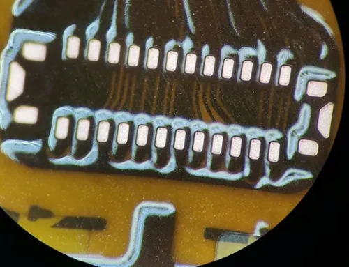
Inner Layer Circuits: Etching the First Circuit Layer
Input: Substrate sheets after cutting.
Process: Creating circuits on the inner layer of copper foil. Apply dry film, expose, develop, etch, and remove the film. “Etch” the designed circuit pattern onto the copper foil.
Output: Inner core board with circuit patterns.
Key Control Points: Line width and spacing accuracy, etching factor, and registration accuracy.
Who is your internal customer? The lamination process.
If your inner layer circuit process is “just good enough,”: Circuit gaps or short circuits cannot be repaired after lamination; line widths out of tolerance lead to uncontrolled characteristic impedance.

Lamination: Putting on the “First Layer of Protection”
Input: Core boards with completed inner layers, along with cover film (CVL), bare laminate, or reinforcement sheets.
Process: Bonding the cover film or reinforcement material to the circuit surface via hot or cold pressing. The cover film provides insulation and protects the circuits, while reinforcement sheets add localized thickness to facilitate component insertion or enhance rigidity (this process is typically scheduled after the outer layer circuit fabrication and cover film lamination, and is considered a post-processing step).
Output: A semi-finished product with the cover film accurately aligned, free of bubbles, wrinkles, and misalignment.
Key Control Points: Laminating alignment accuracy (typically ≤0.1 mm), laminating pressure, temperature, and time; bubble inspection; and reinforcement panel positioning accuracy.
Who is your internal customer? The lamination process.
If you take a “good enough” approach during lamination: The cover film may be misaligned, covering pads or causing uneven copper exposure; bubbles may form, leading to delamination after pressing; or the reinforcement plate may shift, making assembly impossible for the customer.
Lamination: Bonding Multiple Layers into a Single Unit
Input: Laminated stack-up material (inner core layers + cover film + any other layers).
Process: Place the stacked material into a press; under high temperature and pressure, the adhesive in the cover film flows and cures, permanently bonding all layers together.
Output: A multi-layer, firmly bonded FPC substrate.
Key Control Points: Temperature, pressure, time, vacuum level. Peel strength test.
Who is your internal customer? The drilling process.
If you cut corners during the lamination process: A few degrees lower temperature results in insufficient peel strength and delamination after bending; uneven pressure leads to inconsistent board thickness, making drilling prone to misalignment.

Drilling: Creating Interlayer Vias
Input: Laminated multilayer board.
Activity: Use a CNC drilling machine to drill microvia holes at specified locations, creating pathways for subsequent electroplating. This includes through-holes, blind holes, etc.
Output: Boards with precise hole positioning, smooth hole walls, and no burrs.
Key Control Points: Hole positioning accuracy ±0.05 mm, hole diameter tolerance, drill bit lifespan, broken drill bit detection.
Who is your internal customer? The electroplating process.
If you take a “good enough” approach to the drilling process: Misaligned holes result in uneven copper plating on the hole walls after electroplating; undetected drill bit breakage leads to missed holes; and large burrs cause rough hole walls during electroplating.
Electroplating: Depositing Copper on the Hole Walls
Input: Boards with pre-drilled holes.
Process: First, perform electroless plating (chemical plating) to deposit a thin layer of copper on the hole walls, then electroplate to build up the layer to the required thickness. This ensures electrical continuity between the upper and lower circuit layers through the copper layer on the hole walls.
Output: Boards with a continuous, uniformly thick copper layer on the hole walls, free of voids.
Key Control Points: Solution concentration, temperature, current density, copper plating thickness, and cross-sectional analysis of the hole walls.
Who is your internal customer? The outer layer circuit process.
If you take a “good enough” approach in the plating process: The copper layer on the hole walls will be too thin, causing cracks after bending; the hole walls will lack copper, resulting in an open circuit; or the copper layer will have coarse grains, leading to poor reliability.

Outer Layer Circuits: Etching the Final Circuit Layer
Input: The multilayer board with the plating process complete.
Process: Similar to the outer layer circuit process, this involves creating circuit patterns on the outer copper foil. This may include film application, exposure, development, etching, and film removal.
Output: An FPC with clear outer layer circuits.
Key Control Points: Line width and spacing, registration accuracy (alignment with inner layer holes).
Who is your internal customer? The solder mask process.
If you cut corners in the outer layer circuit process: Circuits may short-circuit or open, causing functional failure; misalignment may result in pad-to-hole misalignment.
Solder Mask: Applying an Insulating Coat to the Circuits
Input: The board with the outer layer circuits completed.
Process: Printing or coating the solder mask ink (in some FPCs, a cover film has replaced the solder mask). Exposure and development expose the pads to be soldered, while the remaining circuits are protected by the insulating layer.
Output: A board with clear pads, a smooth solder mask layer, and no bubbles.
Key Control Points: Solder mask thickness, alignment accuracy, curing parameters.
Who is your internal customer? The surface treatment process.
If you cut corners in the solder mask process: The solder mask is misaligned, covering pads and preventing soldering; bubbles in the solder mask cause the board to crack later; the solder mask is too thin, resulting in insufficient voltage resistance.
Surface Finishing: Clad the Pads in “Golden Armor”
Input: Boards after solder mask application.
Process: Depositing a protective metal layer on exposed pads; the most common is electro-gold (ENIG), though OSP and tin plating are also used. This prevents pad oxidation and ensures solderability.
Output: Boards with bright pads, uniform thickness, and no black pads or nickel corrosion.
Key Control Points: Gold thickness, nickel thickness, black pad inspection, solderability testing.
Who is your internal customer? The forming process.
If you cut corners in the surface treatment process: The gold layer is too thin, causing the pads to oxidize and fail to accept solder; black pads result in cold solder joints after assembly; nickel corrosion causes the pads to peel off.

Forming: Cutting Out the Final Shape
Input: Large sheets of board with surface treatment completed.
Activity: Using a punch press or laser cutter, die-cut or laser-cut the FPC from the large sheet according to the customer’s specified outline. This may include registration holes, stamping holes, etc.
Output: Individual FPCs with precise dimensions, smooth edges, and no burrs.
Key Control Points: Dimensional tolerances, die maintenance, burr control.
Who is your internal customer? The testing process.
If your forming process is “good enough”: Dimensions are out of tolerance, and the customer cannot fit the product; large burrs cause material jams during assembly; misalignment results in cut circuits.
Testing: The Final Check
Input: Individual FPCs after forming.
Activities: Electrical performance testing—checking for open circuits, short circuits, and insulation resistance. May also include visual inspection, characteristic impedance testing, and random reliability testing.
Output: Passed FPCs, labeled with a pass certificate, awaiting packaging and shipment.
Key Control Points: Test fixture accuracy, test program coverage, and isolation of defective products.
Who is your internal customer? GenkunFlex Technology’s end customers—external customers.
If you take a “good enough” approach in the testing process: You may miss open-circuit boards, which will reach the customer and result in complaints and claims; or test probe wear may cause misjudgments, leading to the scrapping of good boards or the release of defective ones.
Why Is the “Process Approach” So Important?
After reviewing these ten major processes, you may have noticed a pattern: each process relies on the output of the previous one. If any single process goes wrong, it will topple all subsequent processes like dominoes.
The core principles of the process approach are:
Identify Processes: Break down GenkunFlex Technology’s FPC production into distinct, clear processes.
Manage processes: Define inputs, outputs, resources, methods, and control points for each process.
Connect processes: Identify the preceding and subsequent processes for each step, establishing “internal customer” relationships.
Improve processes: Continuously optimize each process based on its KPIs (such as Cpk for drilling or yield rate for plating).
Without the process approach, what you see is “a disorganized mess”—someone drills, someone applies copper plating, someone tests, but no one cares about anyone else. With the process approach, what you see is “a chain”—each link is interconnected, and every link creates value for the next.

Everyone Is the Master of Their Own Process
At GenkunFlex Technology, you may be responsible for just one process. But please don’t think your process is “small” or “unimportant.”
If the blanking process is off by 1 mm, all subsequent processes will be affected.
Missing even a single hole in the drilling process cannot be corrected by any subsequent effort in the plating process.
If the testing process misses an open circuit, the customer’s end product will have major issues.
By safeguarding your own process, you safeguard the entire chain. If your process fails, the entire chain breaks.
The process approach isn’t just for engineers to write in documents—it’s for everyone to use in their work. Before you start each day, ask yourself: Where does my input come from? What activities do I need to perform? Who receives my output? How do I know I’ve done it right?
This is the process approach. This is the complete journey of GenkunFlex Technology’s FPCs, from cutting to testing.
Conclusion
At its core, multi-layer FPC manufacturing is not defined by any single advanced process, but by the integrity of the entire process chain.
From the first cut of raw material to the final electrical test, every step operates as both a producer and a customer—receiving defined inputs, executing controlled activities, and delivering outputs that must meet strict criteria for the next stage.
The reliability of the final product is therefore not “built” at the end, but accumulated—step by step—through disciplined execution across the entire workflow.
What distinguishes a high-quality FPC is not just precision in isolated processes like drilling or plating, but consistency in process control, alignment between upstream and downstream requirements, and accountability at every interface.
A deviation of 0.05 mm in drilling, a slight under-cure in lamination, or a marginal plating thickness is not a localized issue—it is a systemic risk that propagates forward and amplifies downstream.
The “process approach” provides the only scalable way to manage this complexity.
By clearly defining process boundaries, control points, and internal customer relationships, it transforms manufacturing from a collection of tasks into a synchronized system.
This is what enables repeatability, traceability, and continuous improvement.
In practical terms: quality is not inspected into FPCs—it is engineered into every process, and protected by every operator.
Ultimately, the journey of an FPC is only as strong as its weakest process. Control the process chain, and you control the outcome.