
Flexible PCB Selection Guide: Choosing Between Single, Double, Multilayer & Rigid-Flex Designs
Flexible printed circuit boards (PCBs), also called flex PCBs, have a layer of copper between two layers of polymer. They connect to one or more rigid PCBs using through-hole technology. Choosing the right form factor is important.
You can choose from single-sided, double-sided, multilayer, or rigid-flex options. This choice involves balancing mechanical, electrical, and cost factors.
1. When to Use Flexible PCBs?
Flexible PCBs excel in designs demanding:
Space & Weight Savings
– Ultra-thin profiles (0.05–0.3 mm) replace bulky ribbon cables.Dynamic Flexibility
– Repeated bending (millions of cycles) in foldable devices or wearable hinges.Single-Piece Assemblies
– Hybrid flex and rigid flex PCB constructions reduce connectors.High-Density Interconnects
– Fine-pitch routing and layer count customization enable compact RF or IoT modules.
Common uses include consumer electronics like smartphones, foldable displays, and smartwatches. Automotive systems also use them for battery management and sensor networks. Medical implants and diagnostics benefit from these technologies, too. In aerospace and avionics, weight reduction and reliability are very important.
2. Types of Flexible PCBs & Comparison
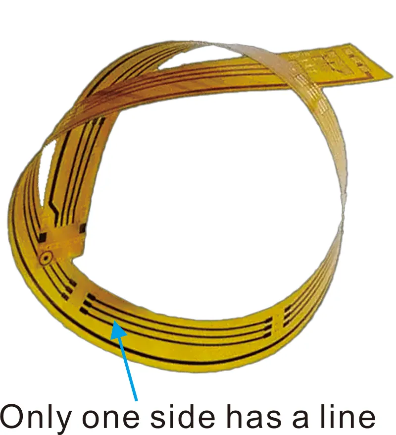
Single-sided FPC
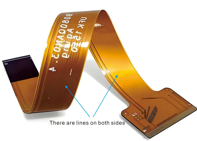
Double-sided FPC
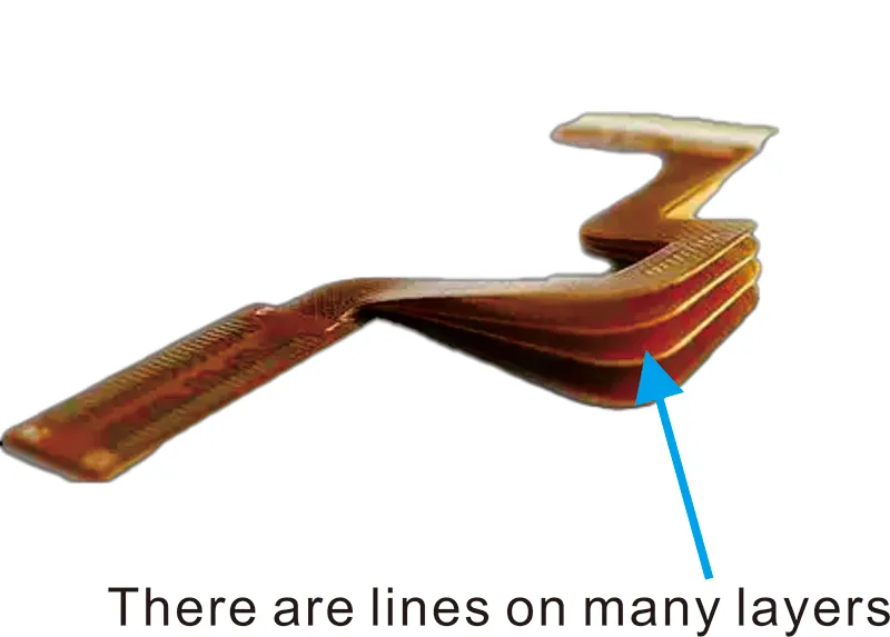
Multilayer FPC
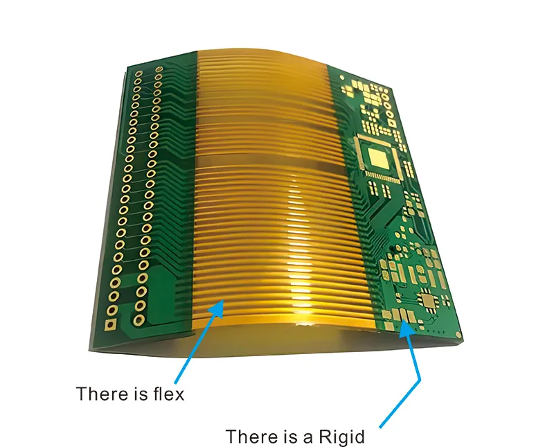
Rigid Flex PCB
Flexible PCBs are categorized by layer count and hybrid designs. Below is a side-by-side comparison:
| Type | Structure | Advantages | Limitations | Typical Uses |
|---|---|---|---|---|
| Single-Sided Flex | One conductor layer on a polyimide circuit board substrate, covered by coverlay or solder mask. | Lowest cost; thinnest flex pcb thickness (0.05–0.2 mm); simplest manufacturing process. | No internal planes; limited routing; low durability in dynamic flex. | Simple signal cables, LED backlighting, static sensor interconnects. |
| Double-Sided Flex | Two conductor layers with plated through holes; PI substrate, coverlay protection. | Enables crossovers; moderate trace density, cost-effective for mid-complexity. | Thicker (0.1–0.3 mm); higher cost vs. single-sided. | LED arrays, moderate-density sensors, semi-flex assemblies. |
| Multilayer Flex | ≥3 conductive layers laminated with adhesive-based materials; internal power/ground planes. | Very high layer count; improved signal integrity; supports high density. | Complex stack-up, strict bend radius rules; highest cost. | RF modules, implantable medical devices, and aerospace electronics. |
| Rigid-Flex PCB | A hybrid of rigid FR-4 sections and flexible PI layers, laminated into one board. | Combines rigid mounting zones with flex regions; eliminates connectors; robust. | Very high cost; complex flex PCB design guidelines, specialized tooling. | Laptop hinges, foldable smartphones, military/avionics. |
3. Materials, Bend Radius & Layer Count
Reference post: How to Choose the Right Flex Material for Your PCB
3.1 Substrate & Conductor Materials
Polyimide (PI): Industry standard; thermal stability to 300 °C; excellent durability.
Polyester (PET): Lower cost; suitable for static or low-stress applications.
PCT (SK Chemicals): Emerging low-loss substrate ideal for high-speed automotive & 5 G.
Copper Type: Use rolled annealed copper for dynamic flex (better ductility); standard electrodeposited copper for static flex.
3.2 Bend Radius & Flex Life
Rule of Thumb:
Static flex: radius ≥ 6× board thickness (single-layer); ≥ 10× thickness (multilayer).
Dynamic flex: radius ≥ 20× thickness; use coverlay, avoid sharp corners.
Exceeding min. Bend radius prevents copper fatigue and cracking.
3.3 Layer Count & Stack-Up
Single/Double: 1–2 layers; simple dielectric bonding.
Multilayer: 4–8 layers typical; uses adhesive-based materials or direct lamination.
Rigid-Flex: Combine 2–12 flexible layers with rigid FR-4; precise lamination sequences crucial.
High Density: More layers allow embedded planes, controlled impedance, and smaller trace/spacing.
4. Design Guidelines & Software Tools
4.1 Flex PCB Design Rules
- Trace Geometry: Use curved traces; avoid 90° corners.
- Component Placement: Mount heavy components on rigid sections to prevent solder joint fatigue.
- Clearance & Spacing: Define based on intended copper thickness and substrate permittivity.
- Coverlay and solder mask serve different purposes. Coverlay is a polyimide film used in dynamic areas. Solder mask is better for static or semi-flex regions.
4.2 Design Software
- Altium Designer: Comprehensive flex and rigid flex PCB support, advanced stack-up editor.
- Cadence Allegro: Robust multi-board and rigid-flex capabilities.
- Frontline InPlan™Flex: Optimizes flex-specific DFM workflows and material libraries.
5. Manufacturing Process & Quality Control
Reference post: PCB Testing: 8 Essential Methods for Quality Assurance (2025 Update)
Base Material Preparation
– Clean and plasma-treat PI to enhance adhesion.Copper Lamination
– Laminate rolled annealed copper for flex regions, electrodeposited for static.Patterning
– Photolithography etches traces; maintain tight design rules for fine-pitch.Coverlay/Solder Mask Application
– Bond coverlay film; apply solder mask where applicable.Drilling & Via Formation
– Laser or mechanical vias; ensure clean annular rings.Rigid Section Integration (Rigid-Flex)
– Laminate FR-4 stiffeners; control warp by matching CTE.Testing & Inspection
– Automated Optical Inspection (AOI) for defect detection; impedance testing within ± 10 %.Dynamic Bend Testing
– Verify flex life cycles using standardized bend-fatigue rigs.
6. Flexible vs. Rigid-Flex PCBs
| Aspect | Flexible PCB | Rigid-Flex PCB |
|---|---|---|
| Structure | Entirely flexible PI substrate | Hybrid PI + FR-4 stiffeners |
| Cost | Lower initial cost | Higher due to hybrid lamination and tooling |
| Manufacturing | Standard flex processes | Requires rigid-flex stack-up equipment |
| Durability | Moderate (static/dynamic flex zones) | High (rigid sections protect components) |
| Use Cases | Wearables, sensors, bendable connectors | Foldable phones, avionics, and complex industrial systems |
7. Industry Applications
| Sector | Use Case | Flex Type |
|---|---|---|
| Consumer Electronics | Foldable smartphones, smartwatches | Multilayer Flex, Rigid-Flex |
| Automotive | Battery management, dashboard controls, sensors | Double-Sided, Multilayer |
| Medical Devices | Implantables, diagnostic probes | Single-Sided, Multilayer |
| Aerospace & Defense | Satellite avionics, missile guidance | Rigid-Flex, Multilayer |
8. Innovations & Future Trends
AI-Driven Manufacturing: AI reduces defects by ~35 % in flex production, optimizing yield and workflow.
Advanced Substrates: PCT and LCP are gaining traction for low dielectric loss in 5G and automotive high-speed links.
Miniaturization: Ultra-thin rigid-flex stacks enable next-gen foldable devices with near-zero thickness.
Embedded Components: Integration of passive/active components within flex layers for further size reduction.
9. Decision Matrix: How to Choose
| Criterion | Single | Double | Multilayer | Rigid-Flex |
|---|---|---|---|---|
| Budget | Low | Medium | High | Very High |
| Flex Cycles | Static | Semi-flex | Dynamic | Dynamic |
| Routing Density | Low | Medium | Very High | High |
| Connector Reduction | No | No | Maybe | Yes |
| Mechanical Strength | Low | Medium | Medium | High |
| Recommended When… | Simple link | Moderate complexity | High performance | Single-piece assemblies |
Selection Steps:
Define Usage: static vs. dynamic, bend radius requirements.
Assess Density: number of layers needed, fine-pitch routing.
Budget & Volume: balance cost per unit vs. performance.
Supply Chain: Confirm the fabricator’s capabilities in your flex type.
Prototyping & Testing: validate bend-fatigue and electrical integrity.
Conclusion
Choosing the best flexible PCB depends on your needs. Consider if you need single-sided, double-sided, multilayer, or rigid-flex. Think about the mechanical demands, electrical complexity, and your budget.
By following proven flex PCB design guidelines, engineers can maximize the potential of flexible circuits. These guidelines include bend radius, material choice, layer count, solder mask versus coverlay, and rolled annealed copper.
Using advanced flexible PCB design software helps engineers achieve this goal for future innovations. Work with an experienced fabricator to make sure your design moves smoothly from idea to production. This will help you get reliable, high-performance, flexible PCBs that meet your specific needs.


Leave A Comment