Double-Sided Flex PCB
Gekun specializes in Flexible PCBs, rigid-flex PCBs, and advanced assemblies, serving clients from startups to global tech companies across communications, computing, automotive, medical, and industrial sectors.
Double-Sided Flex PCB: The Ultimate Guide
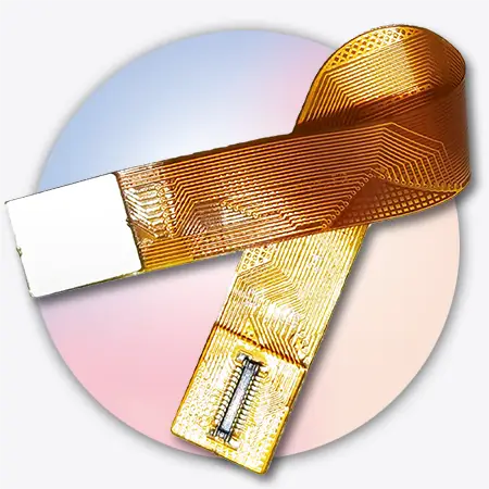
A double-sided flexible PCB is a printed circuit board. It has copper layers on both sides of a flexible polyimide base. These two conductive layers connect electrically through plated through holes (PTHs).
Double-sided flex circuits have two layers of copper. This gives them more routing options and better performance.
They also support a higher density of components compared to single-sided circuits. Their flexibility lets them bend and twist without breaking. This makes them perfect for small and active uses that need reliable connections, like wearables, laptops, and car sensors.
Double-sided flexible PCBs have similar electrical performance to rigid PCBs. However, they greatly reduce wiring complexity and save space. This is especially useful in high-density electronics.
Tip: The difference between him and the double-sided PCB is that the double-sided flex PCB uses flex material. In contrast, the double-sided PCB uses rigid material.
Double-Sided Flexible Circuit Stack-Up
The layer structure of a double-sided flex PCB is key to ensuring mechanical flexibility and signal reliability. Below is a standard flex circuit design stack-up: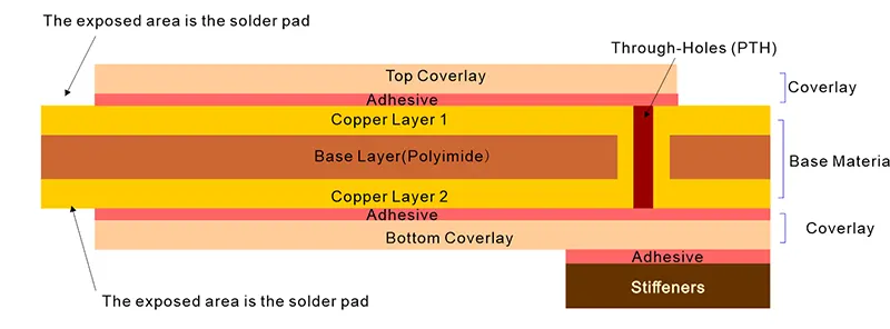
| Layer | Description |
|---|---|
| Top Coverlay | Polyimide insulating material; replaces solder mask in rigid PCBs |
| Copper Layer 1 | Top-side circuit traces for signal and power routing |
| Flex Core | Flexible polyimide dielectric (0.5–4 mil thickness) |
| Copper Layer 2 | Bottom-side circuitry |
| Bottom Coverlay | Protective insulating material for electrical shielding |
| Stiffeners (Optional) | Rigid reinforcements to support component assembly and improve heat dissipation |
Manufacturing Process of Double-Sided Flex Circuit
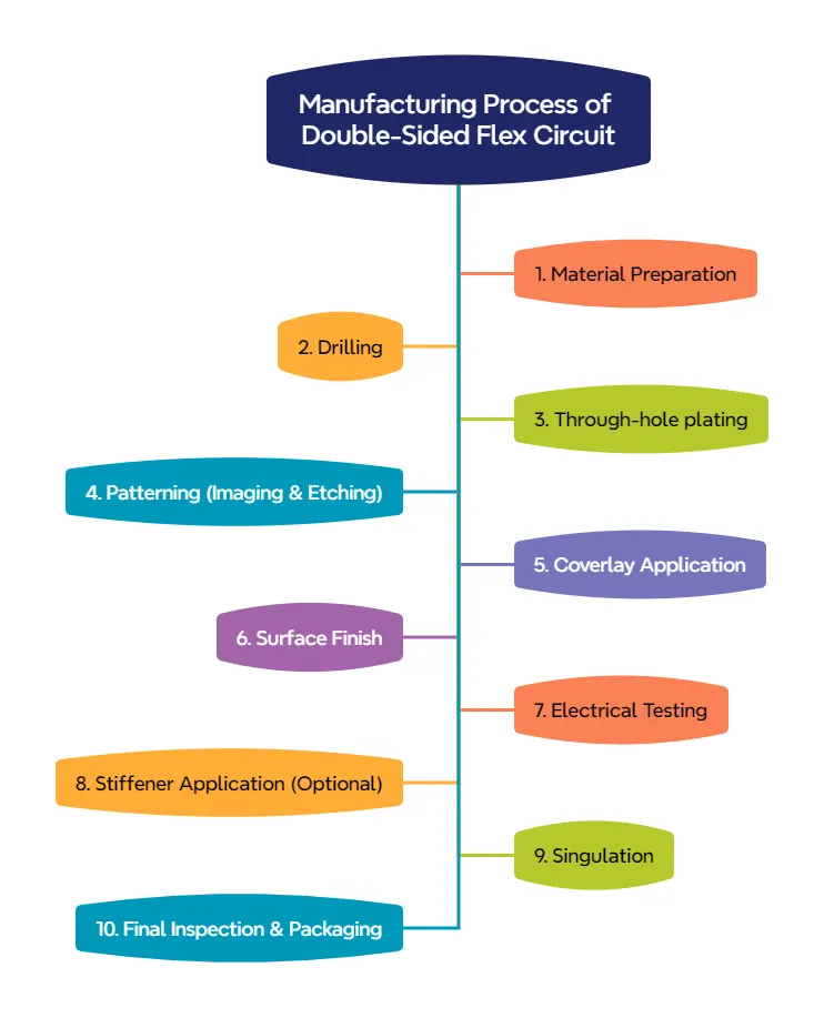
Manufacturing Process of Double-Sided Flex PCB
Manufacturing double-sided flex circuits requires precision and specialized processes:
Material Preparation: The flexible polyimide core, copper foil, coverlay films, and adhesive systems are prepared.
Drilling: Micro-vias and PTHs are drilled through the flexible core material using precise mechanical or laser-cut techniques. Laser drilling is essential for very small vias.
Through-hole plating: The drilled holes are metallized (plated with copper) to create electrical connections between the future top and bottom layers. This step is critical for reliability.
Patterning (Imaging & Etching): A photoresist is applied to both sides of the copper-clad core. Circuit patterns are exposed using UV light through photomasks. The unexposed resist is washed away, and the exposed copper is etched off, leaving the desired circuit traces on both sides. The remaining resist is then stripped.
Coverlay Application: Coverlay films, precisely laser cut to expose solder pads and vias, are laminated onto both sides of the patterned core using heat and pressure (and adhesive).
Surface Finish: Exposed copper pads (for component soldering and connections) receive a protective and solderable finish (like ENIG – Electroless Nickel Immersion Gold, HASL, or Immersion Tin/Silver).
Electrical Testing (Flying Probe or Fixture): Each circuit is rigorously tested for electrical continuity (opens) and shorts.
Stiffener Application (if needed): Pressure-sensitive adhesives (PSA) or thermally cured adhesives are used to bond stiffeners precisely to designated areas.
Singulation (Cutting Out): Individual circuits are cut from the larger production panel using precision routing or laser cutting.
Final Inspection & Packaging: Circuits undergo visual and dimensional inspection before careful packaging to prevent damage during shipping.
Key Materials & Technical Capabilities
Choosing the right materials is critical for performance, flexibility, and cost control in double-sided flex PCB design. Below is an overview of essential parameters and how they affect your circuit’s reliability:
| Parameter | Specifications | Design Impact |
|---|---|---|
| Copper Thickness | 1/3OZ(12 µm), 1/2OZ(18 µm), 1OZ(35 µm), 2OZ(70 µm), 3OZ(105 µm), 4OZ(140 µm) | Thinner copper thickness improves flexibility; thicker copper handles more current |
| Polyimide Thickness | 1/2mil(12 µm), 1mil(25 µm), 2mil(50µm), 3mil(75 µm), 4mil(100µm) | Thinner for tight bends; thicker for mechanical strength in multi-layered builds |
| Board Thickness | 0.10 mm – 0.44 mm | Important for compact builds in multi-layer flex applications |
| Minimum PTH Size | 0.10 mm (4 mil) | Enables dense interconnections and finer routing |
| Min Line/Space | 2 mil / 2 mil (with 0.5 OZ copper) | Supports surface-mounted components and miniaturized layouts |
| Impedance Control | 50Ω, 90Ω, 100Ω + custom options | Required for high-speed signal transmission and signal integrity |
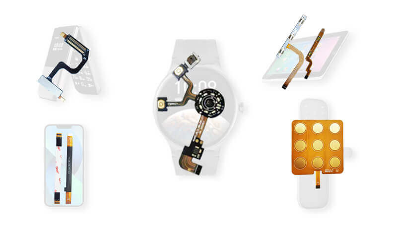
Critical Applications
Double-sided flexible printed circuits are ideal for dynamic environments and compact electronics. Their versatility and reliability make them essential in many applications requiring high performance and space efficiency.
Consumer Electronics
Smartphones: Double-layer circuits power folding mechanisms and display connections
Wearables: Ultra-thin polyimide (0.5 mil) enables comfortable, flexible sensor designs
Laptops: Used in hinge zones, capable of withstanding over 5,000 bends
Industrial & Automotive
Robotics: Boards offer enhanced heat dissipation in compact actuators
Automotive Sensors: Withstand vibration and temperature changes better than rigid PCBs
LED Lighting Systems: Allow compact, bendable assemblies in tight spaces
Medical & Aerospace
Imaging Devices: Flexible PCBs route signals in ultrasound probes and scanners
Implantable Tech: Thin, multi-layered flex designs ensure reliability under sterilization
Military Equipment: High bend-cycle life required in radar modules and avionics
Whether it’s a smartwatch or a space probe, flex circuit design delivers where rigidity fails.
In summary, if you have Double-sided flex PCB needs, we can help.
Material Science Insights
The performance of any flexible PCB starts with its core materials, especially copper thickness and insulating material. These determine how well the board bends, handles heat, and resists stress in critical applications.
Polyimide: The Industry Gold Standard
Thermal Resistance: Withstands up to 400°C
Chemical Stability: Ideal for medical and industrial settings
Dielectric Control: Maintains signal integrity in high-speed environments
Copper Foils: More Than Just Conductors
Rolled Annealed (RA) Copper: Best for multi-layer flex designs requiring durability
Electro-Deposited (ED) Copper: Lower cost option for static or single-sided flex boards
Proper material matching enables manufacturers to meet the unique needs of applications requiring high reliability, miniaturization, or extreme temperatures.
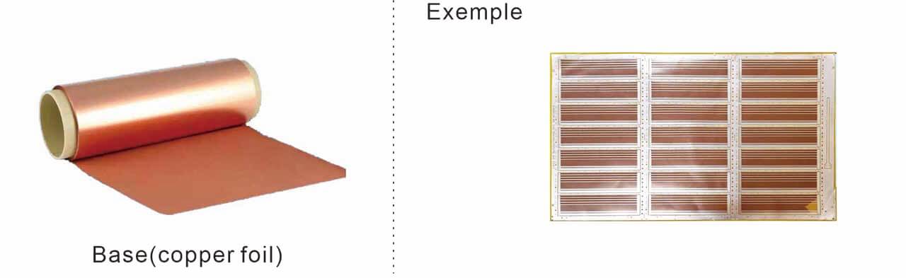
Copper foil ——Flexible printed circuit boards (FPC)’s fundamental material is Copper foil. We press copper foil onto PI film to create the substrate, then etch it to form a conductive pattern, This allows the circuit to transmit signals and electricity efficiently.
——————————————————————————————————————————————————————————————-
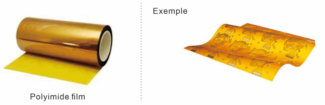
Polyimide film—— It has good mechanical properties and high-temperature resistance,
and withstanding the deformation of flexible circuits during use, like bending and stretching, twisting. Additionally, well it maintains stability and reliability in high-temperature environments.
——————————————————————————————————————————————————————————————-

PI Stiffeners, Steel sheet Stiffeners, and FR4 Stiffeners are used in flexible circuits to enhance mechanical strength and stability. They act as supporting materials, laminated on one or both sides of the circuit board, providing extra support and stability. During use, PI Stiffeners reduce bending and twisting, minimizing damage and failure. Additionally, they offer extra protection, preventing damage and wear during operation.
——————————————————————————————————————————————————————————————-
 double-sided adhesive—— plays a role in providing mechanical support and stability in flexible circuits, bonding the circuit board firmly with other components to ensure reliability and stability.
In summary, if you have flexible circuit design or flexible printed circuit board needs, we can help.
Smart Cost Reduction Strategies
Over 50% of global flexible PCB production consists of double-sided flex circuits. Their popularity comes from their performance-to-cost ratio. That said, cost control is vital, especially for high-volume consumer electronics.
Here are proven strategies to reduce manufacturing costs without compromising quality:
Strategic Material Selection
Different copper types offer varying levels of flexibility, peel strength, and cost. Choose based on your application:
| Material Type | Bend Cycles | Peel Strength | Cost Index | Recommended Use |
|---|---|---|---|---|
| Adhesive ED Copper | 50–100 | 5–7 lb/in | $ | Entry-level, static, flexible PCBs |
| Adhesive-less ED | 100–200 | 8–10 lb/in | $$ | Moderate flexing, consumer electronics |
| Adhesive RA Copper | 500+ | 6–8 lb/in | $$$ | Dynamic medical devices, wearable tech |
| Adhesive-less RA | 1,000+ | 10–12 lb/in | $$$$ | Military and harsh-environment applications |
Gekun Pro Tip: For cost-sensitive builds, 1/2 OZ adhesive ED copper reduces copper cost by up to 30% compared to RA copper.
Coat Thickness vs Impedance Cost
The thickness of polyimide layers also affects impedance control and price:
| Polyimide Thickness | Impedance Tolerance | Cost Premium | Ideal Use Case |
|---|---|---|---|
| 0.5 mil | ±20% | Base Cost | Low-frequency (≤1 GHz) signals |
| 1 mil | ±10% | +15% | High-speed DDR4 or data applications |
| 2 mil | ±7% | +30% | 5G/mmWave circuits and high-speed PCBs |
Gold Plating Optimization
Gold thickness can impact the final board cost drastically. Match it to your requirements:
Selective ENIG (0.05–0.1 μm): Cost-effective for edge connectors
Standard ENIG (0.15–0.2 μm): Used for BGAs and SMT pads
Thick ENIG (>3 μm): Required for gold wire bonding in aerospace and medical
Cost Alert: Full-board thick gold plating can increase cost by up to 200% vs selective ENIG.
Panel Utilization Maximization
Efficient use of PCB panels directly impacts material cost and yield. Here’s how to improve:
Nested Panel Design: Arrange irregular outlines like a puzzle to minimize waste
Unified Stiffener Layout: Use consistent stiffener shapes across designs
Breakaway Tab Optimization: Use laser-cut mouse bites to reduce routing time by 40%
Mixed Technology Panels: Combine rigid-flex PCBs and pure flex circuits to share tooling and panel space
Gekun Case Study: Our proprietary nesting software increases panel yield by 22% during mass production for consumer electronics.
Design & Process Simplification
Sometimes, small design changes can bring major savings:
Remove Silkscreen Layer
When to remove: If component IDs can be etched directly into the copper layer.
Savings: 15–30% panel cost reduction by eliminating printing and curing.
Drill Hole Optimization
Cost Threshold: Avoid exceeding 100,000 holes/m² to prevent added cost per hole.
Tip: Use 0.15 mm holes instead of 0.10 mm where tolerable.
Gold Area Reduction
| Gold Coverage Area | Cost Increase | Solution |
|---|---|---|
| <10% | Base | Use selective ENIG plating |
| 10–20% | +25% | Switch to ENEPIG on contact points |
| >20% | +40–60% | Use immersion tin where possible |
Trace Width Optimization
Avoid: Traces thinner than 0.05 mm—these increase the defect rate significantly.
Design Rule: Use ≥0.08 mm (3 mil) for non-critical signals.
Conclusion
Double-sided flex PCBs strike the perfect balance between complexity, flexibility, and cost. They offer more routing freedom than single-sided flex, yet are simpler and less costly than multi-layer flex options.
By selecting the right materials, such as copper thickness and polyimide layers, engineers can improve their designs. They should also follow good flex circuit design rules. This will help achieve better results
Reduce cost by up to 45%
Improve electrical reliability
Enable next-generation product miniaturization
For projects where rigid PCBs or only one layer won’t meet design or mechanical needs, double-sided flex boards are the best choice.
At Gekun, we specialize in producing high-yield, cost-efficient multi-layered flexible PCBs for industries including consumer electronics, automotive, and medical devices.

