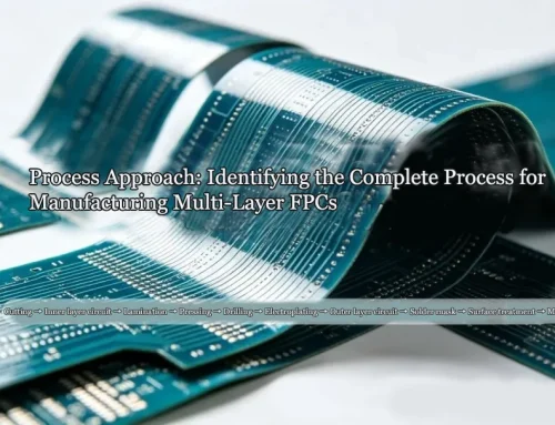
PCB Etching Process: Flexible PCB & Rigid Flex Manufacturing
PCB Etching Process: Flexible PCB & Rigid Flex Manufacturing
Introduction
The etching task in PCB design is one of the most important steps in making printed circuit boards. It directly influences the precision of the circuit trails, hence performance, as well as the life of the end product.
Accurate etching is important. It is used to create a standard stiff board. It is also used for flexible and rigid designs. Additionally, it is essential for making a flexible printed circuit (FPC). This helps keep the copper traces free of defects and ensures quality.
In the case of flexible PCBs, you need to be more precise with your etchings as compared to those in rigid boards. The thin copper layers and flexible polyimide base are more sensitive to chemical and mechanical stress. Understanding the differences between standard PCB etching and flex PCB etching helps engineers and procurement specialists choose better partners. This knowledge can prevent production delays and ensure good product quality in high-density applications.
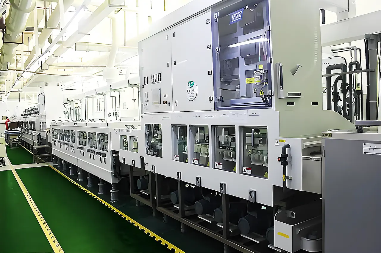
Etching production line
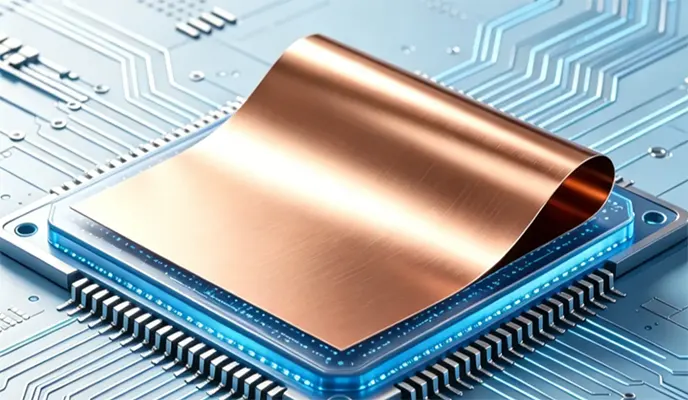
What is PCB Etching?
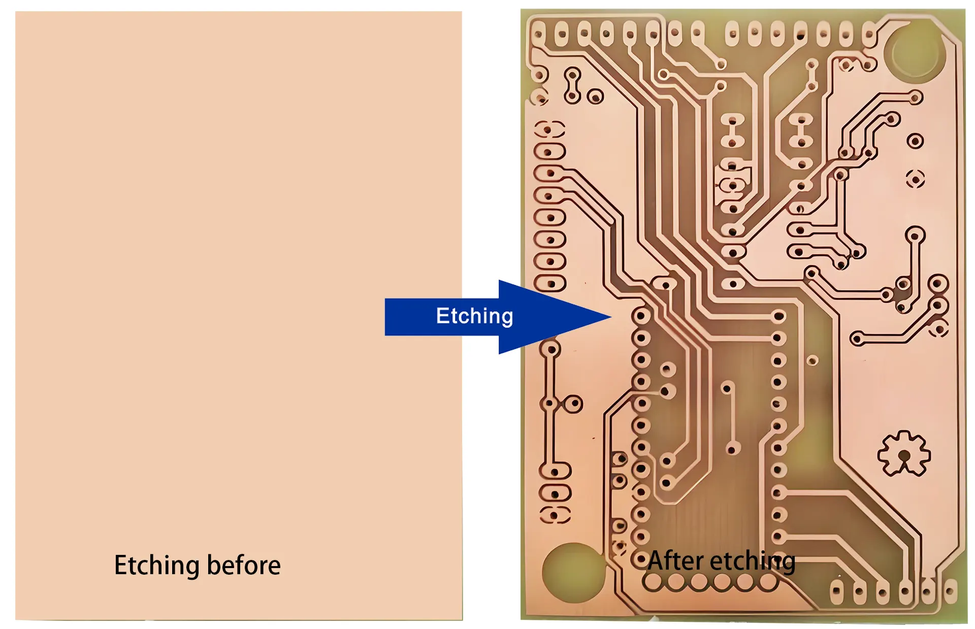
PCB etching is the process of removing unwanted copper from PCBs. This creates the circuit pattern we want. It usually starts by covering the copper surface with a protective photoresist or transfer paper. This masks areas that need to stay conductive. The exposed copper areas are then dissolved using an etching solution.
In most production lines, two common etching methods are used:
| Etching Method | Application | Precision Level |
|---|---|---|
| Chemical Etching | Standard PCBs & Flexible PCBs | Medium |
| Laser Etching | Fine Line & High-Density PCBs | High |
The solutions used for etching are usually ferric chloride or cupric chloride. These chemicals dissolve the copper in unwanted areas. This process is known as chemical etching and is the most common method. The etch rate is controllable by varying the concentration of the chemical, the temperature, and the level of agitation.
Laser etching is often chosen for ultra-fine traces or HDI PCB design, where precision is critical. For flexible printed circuit boards, chemical etching is still the best method. It removes copper evenly and does not harm the substrate
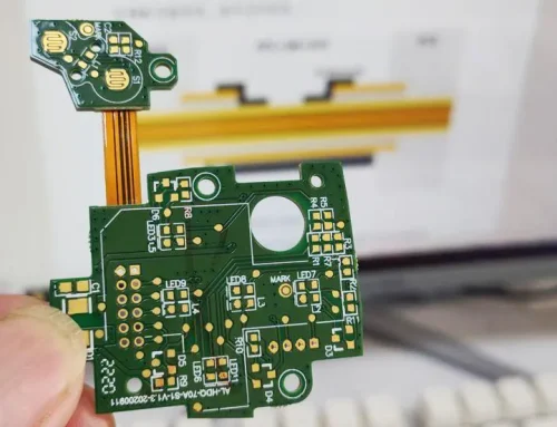
Flexible PCB Etching Process
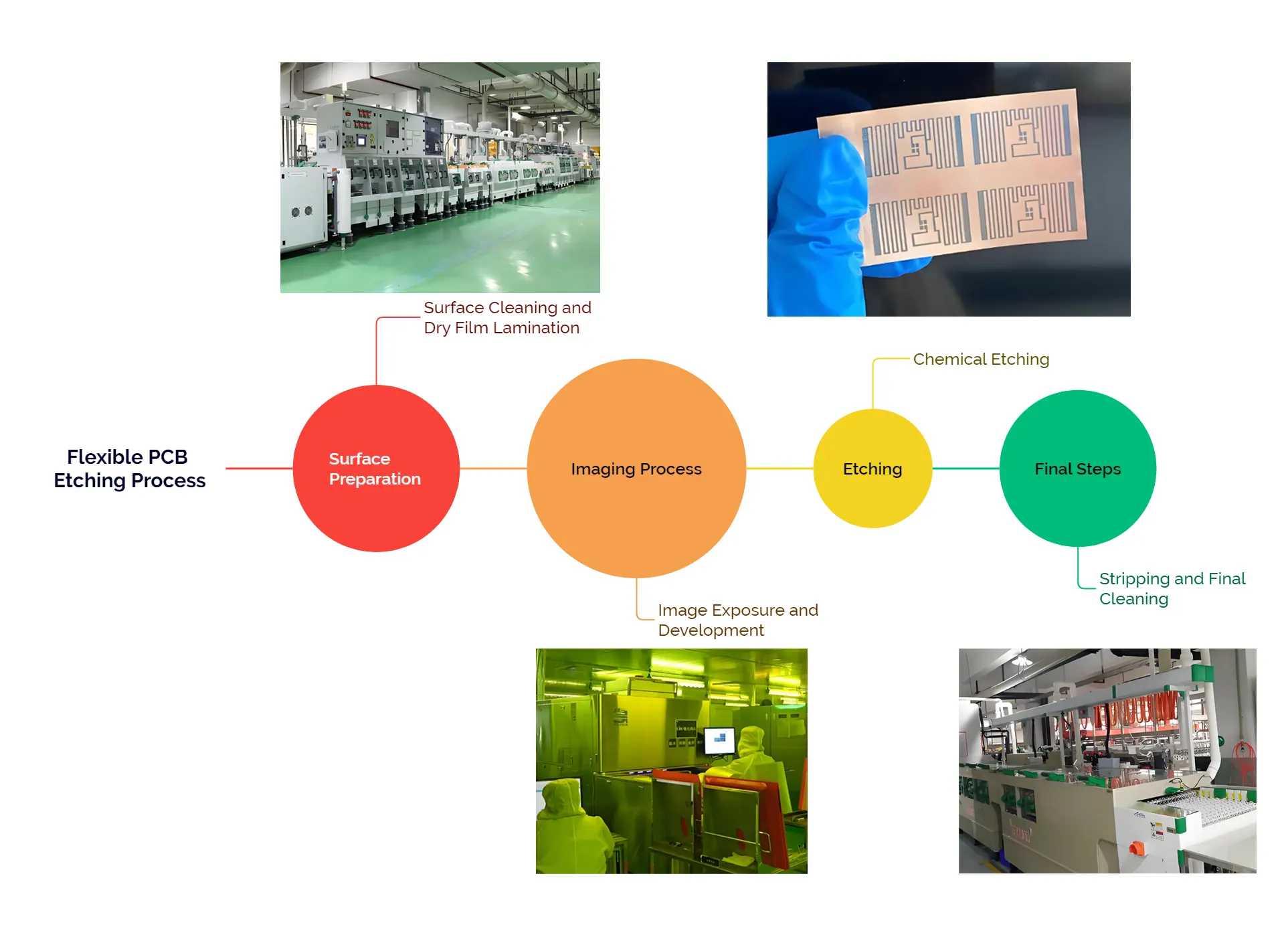
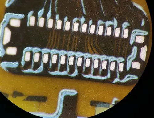
PCB etching process
One key difference in flexible PCB etching compared to rigid boards is the effect on the base polyimide layer. It is important to avoid over-etching or damaging this layer. This can be done by controlling the processes more carefully. Undercutting is a typical issue when it comes to etching copper, especially in the case of copper foils down to 12μm-35μm.
Step-by-Step Process:
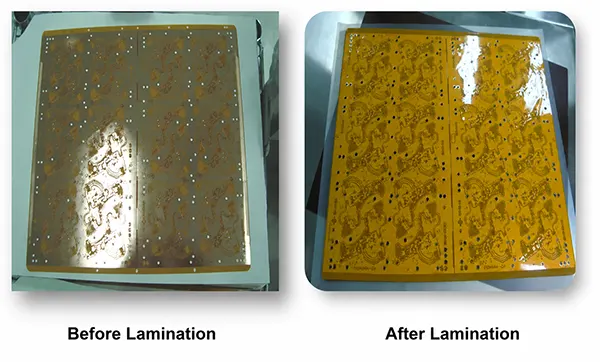
Surface Cleaning and Dry Film Lamination
Remove dust, oils, and oxidation from the copper clad to ensure proper adhesion of the protective layer.
Apply a dry film or transfer paper to protect copper areas that must remain as traces.
Image Exposure and Development
UV light exposure transfers the PCB design pattern to the protective layer.
Development removes unexposed areas, leaving copper exposed for etching.
Chemical Etching
Immerse the panel in an etching solution (commonly ferric chloride or cupric chloride).
Maintain a steady etch rate by controlling chemical concentration, flow, and temperature.
For double-sided and flex and rigid designs, each side may require individual processing to ensure accuracy.
Stripping and Final Cleaning
Remove the protective film to reveal the finished circuit pattern.
Rinse everything really well or the chemical residue will eat through the copper plating and/or affect your conductivity.
Key Factors for High-Quality Etching
Copper Thickness
Thicker copper plates or heavy copper layers require longer etching times, which increases the risk of lateral undercutting.
Designers must properly time flex circuits using thin copper foils (≤ 18μm) to prevent over-etching.
Etching Chemicals and Temperature
The type of etching solution and its temperature directly affect the etch rate and quality.
Consistent agitation improves uniformity and prevents streaks on the surface of the PCB.
Trace Width and Spacing
High-density designs need strict control of lateral etching to avoid shorts or open circuits.
Engineers can use advanced laser processing for ultra-fine features in PCB design.
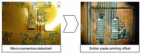
Common Problems and Solutions
| Problem | Cause | Solution |
|---|---|---|
| Over-etching | Excessive chemical exposure | Reduce exposure time or lower chemical strength |
| Uneven etching | Poor chemical flow or contamination | Improve agitation and clean tanks |
| Residual copper | Weak etchant or poor exposure | Check UV alignment and chemical potency |
For PCB board etching, it is important to choose the right drill bit for via preparation. Additionally, keeping clean edges during processing helps improve overall quality.
Conclusion
The PCB etching process is key to the quality of every printed circuit board. It ranges from standard rigid boards to complex flex and rigid designs. Mastering the balance between copper layers, chemical concentration, etch rate, and timing ensures consistent results. For PCB design teams, understanding these parameters not only improves product reliability but also makes production more cost-effective. Additionally, it contributes to faster time-to-market.
Companies can work with skilled manufacturers. These manufacturers understand both flexible and rigid needs. This ensures that each process produces high-quality and reliable circuit boards. These boards meet today’s electronic demands.