PCB Assembly Process: A Step-by-Step Guide
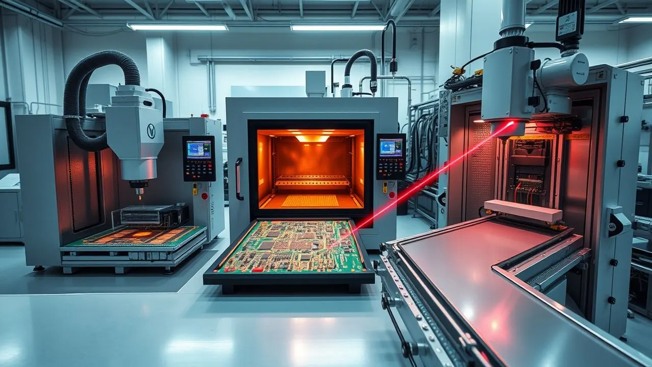
The PCB assembly process (often called PCBA) is the heartbeat of modern electronics manufacturing. Transforming a bare printed circuit board (PCB) into a functional electronic assembly requires precision, expertise, and rigorous quality control.
To understand this process, you need to know more than just the steps. You must also see the key differences between assembling rigid boards and the special challenges of flex PCB assembly.
This guide explains the whole PCB board assembly process. It covers everything from design files to final testing. It also focuses on important details for FPC assembly.
Other related post: Mastering SMT Assembly: Advantages and Future Trends
What is PCB Assembly (PCBA)?
PCB assembly refers to the process of soldering electronic components onto a fabricated PCB. The result is a PCB Assembly (PCBA) – a fully functional circuit board ready for integration into an end product. This stage is distinct from the PCB manufacturing process, which focuses solely on fabricating the bare board.
- Why PCBA is Critical:
- Functionality: Turns a passive board into an active electronic system.
- Value Addition: Components represent the majority of a board’s cost and functionality.
- Reliability: A flawless assembly process directly impacts product longevity and performance. Defects introduced here are costly and can lead to field failures.
- Modern boards, especially those with surface mount components (SMDs), require careful assembly. This includes components like micro-BGAs and fine-pitch ICs. Precise methods are essential for their assembly.
Pre-Assembly Preparation: Setting the Stage for Success
Success in the PCB assembly process begins long before components are placed. Rigorous preparation is non-negotiable:
Design for Manufacturability (DFM) Check:
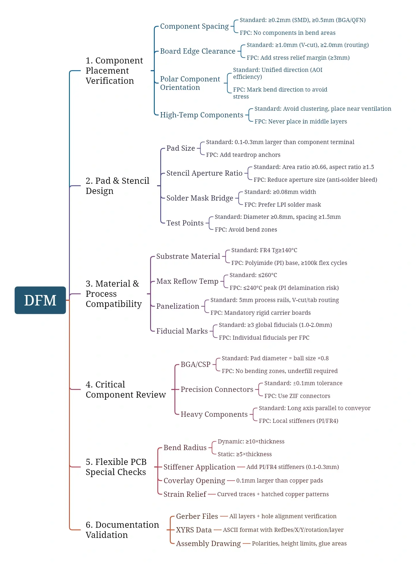
DFM-Detailed
A thorough PCB design DFM review is paramount. This ensures the board can be efficiently and reliably assembled. Checks include component spacing, pad sizing, thermal relief, solder mask (solder mask) clearances, and panelization design.
The flex PCB assembly process requires strict design for manufacturing (DFM) rules. It focuses on bend radii, stiffener placement, and keeping components out of flex areas.
TIP: Missing DFM leads to assembly hell.
Bill of Materials (BOM) Finalization & Component Sourcing:
An accurate, complete BOM listing all electronic components (part numbers, values, quantities, descriptions) is essential. Sourcing components from reliable suppliers prevents delays and counterfeit parts, especially crucial for complex or flex PCB assembly.
PCB Fabrication Review:
Inspect incoming bare boards (rigid or flexible) against Gerber files (design files). Look for defects like shorts, opens, drill errors, or surface imperfections. For flex boards, check polyimide integrity, adhesive coverage, and copper thickness uniformity. This step verifies the PCB manufacturing process output.
Solder Paste & Stencil Preparation:
Selecting the right solder paste (e.g., lead-free SAC305) is vital. A laser-cut stainless steel stencil, aligned with the PCB design, is used to apply paste precisely onto SMD pads. Stencil thickness and aperture design directly impact solder joint quality. Flex boards often require specialized stencils and supporting fixtures during printing.
PCB Baking/Moisture Removal
- Why Bake? PCBs absorb moisture during storage/transport. Unremoved moisture vaporizes in a reflow oven, causing “popcorning” (internal delamination) or solder splatter.
- Standard Baking Process:
Rigid PCBs (FR4): 125°C ±5°C for 4-12 hours (IPC-J-STD-033 standard).
Flex PCBs (PI substrate): 105-110°C for 2-8 hours – Lower temp avoids polyimide brittleness and adhesive degradation.
MSD Handling: Moisture-sensitive components, like BGAs and QFNs, must be stored dry at less than 5% relative humidity. They should be baked separately according to their MSL level, as stated in IPC-J-STD-033, before placement.
The Core PCB Assembly Process Steps
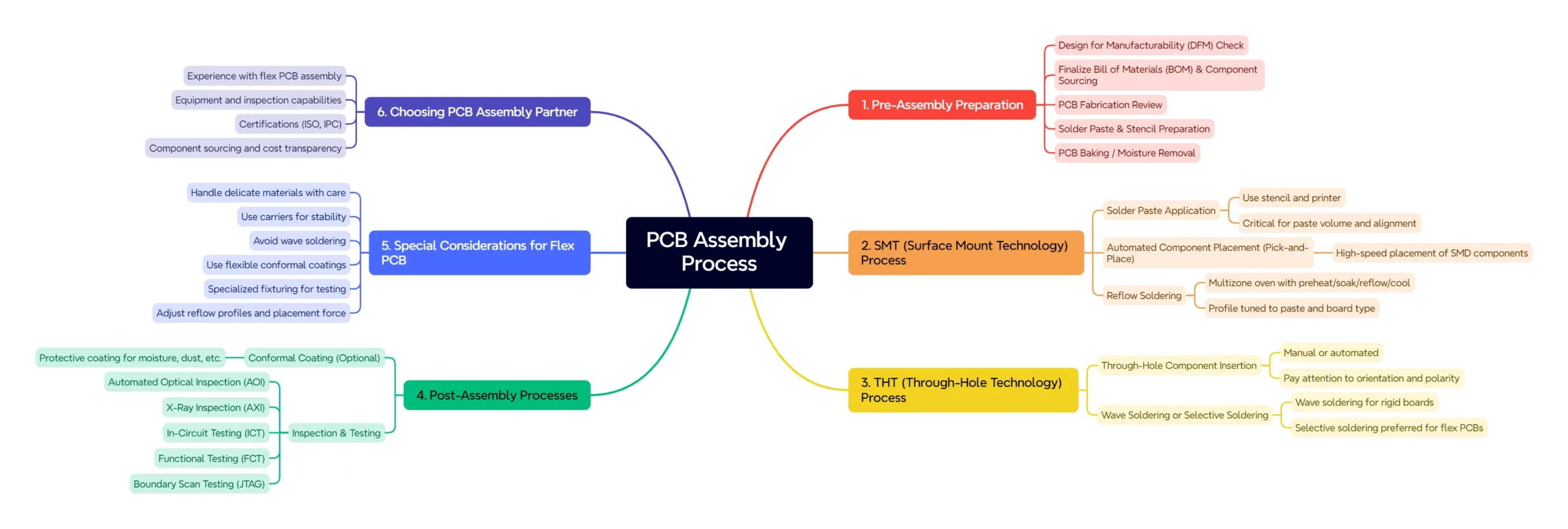
The heart of the PCBA process involves sequential, highly controlled operations. Here’s the standard PCB assembly process flow:
Step 1: Solder Paste Application (SMT)
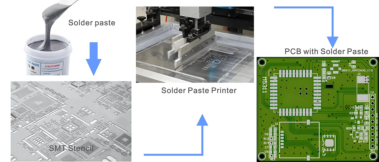
Printing solder paste steps
- Process: Solder paste is precisely printed onto the PCB’s surface mount pads using the stencil and a solder paste printer.
- Key Points: Consistent paste volume, accurate alignment, no bridging or smearing.
- Flex PCB Focus: Needs very fine stencils and special rigid carriers to keep the flexible board flat during printing. Uneven surfaces are a major flex PCB assembly process challenge.
Step 2: Automated Component Placement (Pick-and-Place – SMT)
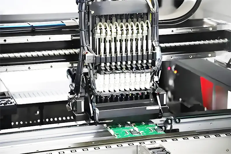
Automated Component Placement
- Process: High-speed pick and place machines accurately pick surface mount components from reels/trays and place them onto the solder-pasted pads.
- Key Points: Extreme precision (micron-level), high speed, handling miniature components (01005, 0.3mm pitch BGAs).
- Flex PCB Focus: Placement pressure must be meticulously controlled to avoid damaging delicate polyimide. Dedicated flex carriers are essential for stability.
- Panelization is important for efficient FPC assembly in automated lines. It uses breakaway tabs or a rigid-flex design. Vacuum nozzles might need adjustment.
Step 3: Reflow Soldering (SMT)
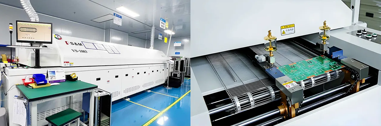
Reflow Soldering
- Process: The PCB goes through a multi-zone reflow oven. It follows a carefully controlled temperature profile. This profile includes preheat, soak, reflow peak, and cooling.
- Key Points: Profile tailored to paste and components; prevents tombstoning, cold joints, voids, or component damage. Critical for reliable solder joints.
- Flex PCB Focus: Polyimide (PI) substrates have lower thermal stability than FR4. Reflow soldering profiles need lower peak temperatures, about 5-20°C lower. They also require shorter dwell times above the liquidus. This helps prevent blistering, delamination, or too much Z-axis expansion. Thermal mass differences within a rigid-flex panel need careful profiling.
Step 4: Through-Hole Component Insertion (THT – Manual or Automated)
- Process: Hole components (connectors, large capacitors, transformers) are inserted into designated holes on the PCB. Can be manual or done by selective insertion machines.
- Key Points: Correct component orientation and polarity. Secure fit before soldering.
- Flex PCB Focus: THT is usually not recommended in pure flex areas. This is because of high mechanical stress during insertion and the risk of pad lifting. If unavoidable (e.g., on rigid sections of rigid-flex), extreme care and potentially specialized tooling are needed. Manual insertion is often preferred for low-volume flex PCB assembly processes.
Step 5: Wave Soldering or Selective Soldering (THT)
- Process:
- Wave Soldering: The bottom side of the board passes over a molten solder wave, soldering all THT leads simultaneously. Requires masking of SMD areas.
- Selective Soldering: A special solder nozzle carefully soldered individual THT joints or connectors. This method is great for mixed-technology boards or heat-sensitive areas.
- Key Points: Flux application, preheat, solder temperature, contact time. Prevents bridging or cold joints.
- Flex PCB Focus: WAVE SOLDERING IS GENERALLY UNSUITABLE FOR FLEXIBLE PCBs! The high temperature and physical force of the wave can easily melt adhesives, delaminate layers, or distort the board.
Selective soldering with carefully controlled settings is the only practical automated choice for THT on flex. Otherwise, highly skilled manual PCB assembly techniques must be used.
Step 6: Conformal Coating (Optional but Recommended)
- Process: A thin protective film made of polymer (like acrylic, silicone, or urethane) is applied. This can be done by spraying, dipping, or brushing. The film protects the assembly from moisture, dust, chemicals, and electrical leakage.
- Key Points: Uniform coverage, masking of connectors/test points, and proper curing.
- Flex PCB Focus: Coating material must be flexible (e.g., silicone-based) to withstand bending without cracking. Application thickness needs control, especially in bend zones, to avoid stress concentration. Masking requirements can be higher for complex flex assemblies.
TIP: SMT uses a mounting process. In this process, components and solder joints are on the same side of the PCB. This allows for high-density automated production using reflow soldering. THT uses a process where component leads go into holes. THT can be used selectively.
Post-Assembly: Inspection, Testing & Quality Control
(PCB Testing: 8 Essential Methods for Quality Assurance (2025 Update)
Robust inspection and testing are non-negotiable parts of a reliable PCB assembly process flow. This is where PCB assembly manufacturers prove their worth.
Automated Optical Inspection (AOI):
High-resolution cameras scan the board. They look for missing parts, misalignment, polarity errors, solder bridges, too much or too little solder, and lifted leads. Essential for high-volume SMT quality control.
X-Ray Inspection (AXI):
Penetrates the board to visualize hidden solder joints under BGAs, QFNs, and within connectors. Detects voids, head-in-pillow defects, insufficient solder, and internal bridging. Critical for complex assemblies and the flex PCB assembly process, where rework is risky.
In-Circuit Testing (ICT):
Uses a bed-of-nails fixture to make electrical contact with test points. Checks for opens, shorts, component values (resistance, capacitance), and basic functionality of individual components/networks. Excellent for catching manufacturing defects.
Functional Testing (FCT):
Powers up the PCBA and simulates its real-world operating environment. Verifies the board performs its intended functions correctly (e.g., communication protocols, signal outputs, power consumption). The ultimate test of fitness for purpose.
Boundary Scan Testing (JTAG):
Primarily for digital circuits. It uses built-in test circuits that follow the IEEE 1149.1 standard. This works on compatible ICs to test connections and core logic. It does this without needing full physical access. Efficient for complex boards.
Flex PCB Focus:
Test fixtures (especially for ICT) must accommodate the flex board’s potential movement or require specialized designs. Connector mating/unmating during the test requires extra care. The flex PCB assembly process may require additional bend cycle testing for dynamic applications.
Special Considerations for Flexible PCB (FPC) Assembly
Flex PCB assembly process introduces unique complexities beyond the standard rigid PCB board assembly process. Partnering with experienced PCB assembly manufacturers specializing in FPC is crucial.
Unique Challenges in FPC Assembly:
- Material Delicacy: Thin polyimide films and copper are easily scratched, torn, or creased. Requires gentler handling throughout the assembly process.
- Dimensional Instability: Flex materials can stretch or shrink a bit more than FR4 when heated or under tension. This can affect registration accuracy during printing and placement. Carrier boards are essential.
- Critical Need for Support: Bare flex boards lack rigidity. Custom carriers and fixtures are needed for every step. This includes printing, placement, reflow, and inspection. They help make a stable, flat work surface. This ensures accuracy in the process.
Panelization is important. Individual flex circuits are usually too weak for automated handling. They are panelized using rigid breakaway tabs or designed as part of a rigid-flex PCB structure for assembly. Depanelization post-assembly requires care.
- Thermal Sensitivity: Lower maximum temperature tolerance necessitates specialized reflow soldering profiles. Wave soldering is prohibited.
- Soldering Challenges: Smaller pads, potential for Z-axis expansion, and sensitivity require precise control during soldering (reflow or selective).
- Cleaning & Handling: Requires compatible, gentle cleaning agents. Operators need specific training to avoid kinking or stressing the boards.
Best Practices for Reliable FPC Assembly:
- Rigorous FPC-Specific DFM: Involve your PCB assembly manufacturer early. Address bend requirements, stiffener locations, component keep-outs, and panelization design.
- Choose an FPC Specialist: Not all PCB manufacturers excel at flex assembly. Look for proven experience and dedicated flex lines.
- High-Quality Materials: Use flex-rated solder paste, coatings, and adhesives compatible with polyimide.
- Invest in Fixturing: High-precision carriers are non-negotiable for quality and yield.
- Optimize Process Parameters: Adjust each step (paste print pressure, placement force, reflow profile, selective solder settings) for flex.
- Enhanced Inspection: Leverage AOI and AXI extensively. Consider more manual visual checks.
Choosing the Right PCB Assembly Partner
Selecting your PCB assembly manufacturer is a critical decision impacting cost, quality, and time-to-market.
- Key Selection Criteria:
- Technical Capability & Expertise: Do they handle your technology (HDI, high-speed, RF)? CRITICAL: Do they have proven flex PCB assembly process experience? Ask for case studies.
- Equipment & Technology: Modern SMT lines, advanced inspection (AOI, AXI), selective soldering, conformal coating. Dedicated flex support systems?
- Quality Systems & Certifications: ISO 9001, IATF 16949 (automotive), ISO 13485 (medical), IPC-A-610 adherence. Robust QC processes.
- Scalability & Volume: Can they handle your prototype, low-volume, and high-volume needs? Services like PCB assembly express for quick-turn prototypes?
- Supply Chain Management: Component sourcing expertise, BOM validation, and counterfeit mitigation.
- Communication & Support: Responsive engineering support, clear communication, DFM feedback.
- Location & Logistics: Impact on shipping costs and lead times.
- Value & Cost: Competitive pricing without sacrificing quality. Understand their cost structure.
- The Flex Imperative: For the flex PCB assembly process, prioritize manufacturers with demonstrable FPC expertise, specialized equipment (carriers, fine-feature stencil capability), and a track record of success. Generic PCB manufacturers often lack the necessary know-how and infrastructure.
I believe Gekun is your best choice.
Conclusion: Mastering the PCB Assembly Process for Success
The PCB assembly process is a sophisticated sequence transforming design intent into functional electronics. Understanding each step is important. This includes DFM, component placement with a pick and place machine, and reflow or wave soldering. It also covers inspection methods like automated optical inspection (AOI) and X-ray. Finally, rigorous testing is essential.
For flexible PCB assembly, acknowledging and expertly managing the unique material, thermal, and handling challenges is paramount to achieving reliability. Choose the right PCB assembly manufacturer with the right skills, especially for flex.
Follow best practices and use strict quality control. This way, your PCBA will meet high standards for performance and durability. It will help create successful electronic products.
Frequently Asked Questions (FAQs) about PCB Assembly Process
Basic Concepts
Q: What’s the difference between PCB and PCBA?
A: A PCB (Printed Circuit Board) is the bare, unpopulated board. PCBA (Printed Circuit Board Assembly) is the PCB after all electronic components have been soldered onto it.Q: What is SMT in PCB assembly?
A: SMT (Surface Mount Technology) is the main process for PCB assembly. In this method, components are placed and soldered on the board’s surface, mainly using a pick and place machine and a reflow oven. Contrasts with Through-Hole Technology (THT).Q: What files do I need to provide for PCB assembly?
A: Essential design files include: Gerber files (for board fabrication), Bill of Materials (BOM), Pick-and-Place file (XYRS data), Centroid file, Assembly Drawings, and any specific test procedures.Q: Where can I find a PCB assembly process flowchart or video?
A: Many reputable PCB assembly manufacturers provide PCB assembly process flowchart diagrams or videos on their websites. Search for “pcb assembly process pdf”, “pcb assembly process ppt”, or “pcb assembly process video” online.Q: Can you assemble both rigid and flexible boards?
A: Yes, experienced manufacturers often handle both rigid and flex PCB assembly processes, including complex rigid-flex assembly. Ensure they explicitly state expertise in FPC assembly.
Technical & Practical
Q: How long does the PCB assembly process take?
A: Turnaround time varies based on complexity, component availability, order volume, and the manufacturer. Simple prototypes can take days; complex high-volume builds take weeks. Flex PCB assembly often takes longer due to specialized handling.Q: What are the common defects in PCB assembly?
A: Common defects include solder bridges, insufficient/excess solder, tombstoning (chipped components), missing/misaligned parts, cold solder joints, voids (detected by X-ray), and lifted pads. Rigorous AOI and testing catch these.Q: What are the biggest challenges in assembling flexible PCBs?
A: Key challenges involve handling delicate materials, dimensional stability requiring rigid carriers, lower heat tolerance needing specialized reflow profiles, the unsuitability of wave soldering, and ensuring reliability in bend areas. Specialized manufacturers are essential.Q: How much does PCB assembly cost?
A: Cost depends on board complexity (layer count, size), component count/type/cost, volume (NRE setup vs. per-unit), labor (manual vs. automated), testing requirements, and the manufacturer. Flex PCB assembly typically costs more due to specialized processes.


Leave A Comment