
Flexible PCB Material Preparation: Cutting and Cleaning Process
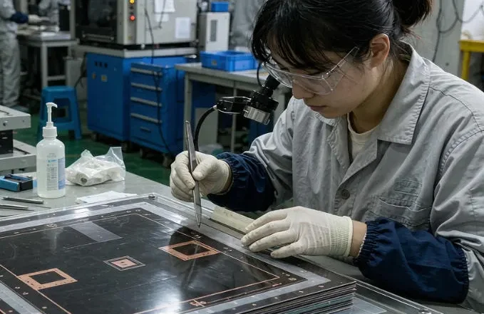
Flexible PCB material preparation is the first production step in flex manufacturing. It covers incoming inspection, polyimide base material preparation, cutting to panel size, edge trimming and surface cleaning. Done well, it protects yield in etching, lamination and coverlay alignment. This guide explains the materials, cutting methods, flex PCB cutting cleaning controls and inspection criteria.
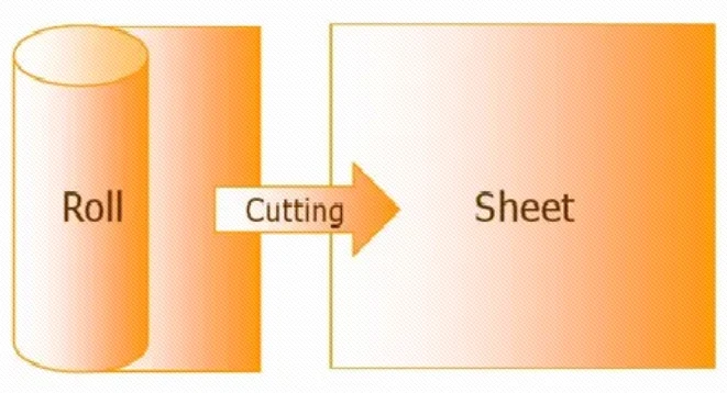
Flexible PCB Material Cutting
Most flexible circuit boards are cut from roll stock. Each panel is cut to the size defined by the manufacturing instruction (MI). Small errors at this stage travel downstream. A rough edge distorts registration during etching. A contaminated surface weakens adhesive bonds. Therefore, preparation must be strict and repeatable, not approximate.
Materials and Polyimide Base Material Preparation
Flexible Circuits use a small set of core materials. Each one behaves differently under a blade, a laser or a router. In practice, the material list is also the cutting list.
| Material | Function | Notes for cutting and prep |
|---|---|---|
| Polyimide film | Flexible substrate and base material | Standard choice for thermal stability and flexibility |
| Copper foil | Conductive traces | Thickness varies by design and current needs |
| Adhesive layer | Bonds copper to substrate | Critical for multilayer and rigid-flex stacks |
| Coverlay / solder mask | Protects traces and pads | Coverlay for flex; solder mask on some rigid-flex areas |
| Stiffener (FR-4 or PI) | Adds rigidity at connector and SMT zones | Positioned after the main panel is prepared |
These flexible materials form the backbone of any Flexible PCB. Teams prefer polyimide-based materials when they need flexibility plus heat resistance.
Polyimide base material preparation
Polyimide base material preparation is more than unrolling film. PI picks up moisture from the air. Trapped moisture flashes into steam during lamination. That causes delamination and solder defects later. Therefore, films are baked before use when humidity control alone is not enough.
Roll-to-roll feeding suits thin, high-volume film. Sheet-fed loading suits thicker stacks and small batches. Both need clean handling, because one particle under the coverlay becomes a reject.
Substrate comparison for cutting
| Substrate | Typical strength | Cutting consideration |
|---|---|---|
| Standard PI film | Heat resistance and flexibility | Cuts cleanly with shear, laser or routing |
| Two-layer PI (adhesiveless) | Thinner stack, longer bend life | Less adhesive squeeze-out, so edges stay clean |
| LCP | Low moisture uptake, stable at high frequency | Needs sharp tooling; heat-sensitive at the cut line |
| Halogen-free substrate | Environmental compliance | Similar handling to PI, but verify the bake profile |
For layer-by-layer choices above this base film, see Flexible PCB Material Stack-Up.
Step-by-Step Material Preparation Workflow
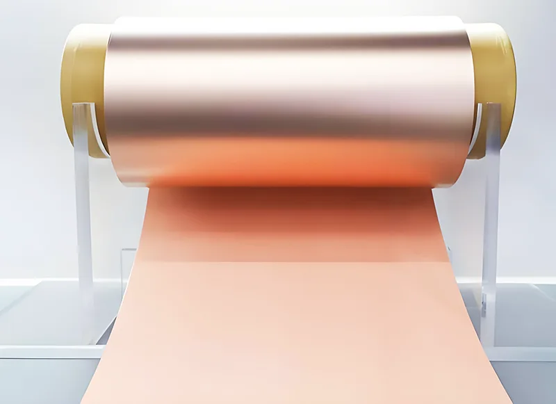
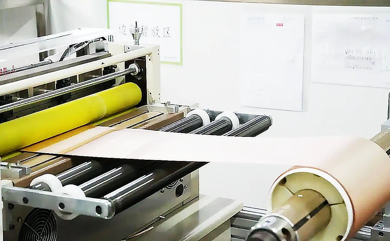
Flexible PCB roll
Production teams follow a fixed sequence. Each step has written acceptance criteria.
1. Incoming inspection. Verify copper thickness and surface finish. Confirm polyimide sheets match the spec. Check for coating defects and contamination.
2. Conditioning and drying. Bake polyimide films when needed to remove moisture. Record bake time and temperature.
3. Cutting to panel size. Cut panels to production dimensions before lamination. Use precision flex PCB cutting to hold tolerances.
4. Fiducial marking. Add fiducials and registration points for later steps.
5. Edge trimming and beveling. Remove oxidized or uneven edges. Beveled edges improve alignment in lamination and drilling.
6. Surface cleaning. Remove oils, particulates and residues before the panel moves on.
7. Final inspection and storage. Check for micro-scratches and particulates. Store in dry, controlled conditions.
Each step in the manufacturing process needs a clear acceptance criterion. Record measurements so the lot stays traceable.
Technical Specifications and Standards
Set measurable acceptance criteria before the first panel is cut. A practical specification sheet for flexible PCB material preparation should state:
- Panel size tolerance: ±0.10 mm for laser or routing, ±0.20 mm for shear on simple panels.
- Fiducial position: ±0.05 mm from nominal; datum edges square within 0.10 mm per 100 mm.
- Edge quality: burr height ≤50 µm; no loose stringing longer than 0.10 mm; laser char zone ≤0.10 mm and not bridging traces.
- Cut depth into carrier: 0.02–0.05 mm where partial-depth cutting is used; no nicks in underlying copper.
- Cleanliness: no visible particles >50 µm at 10x; tape-lift particle count within the agreed limit; final DI rinse resistivity ≥1 MΩ·cm; surface energy ≥38 mN/m before lamination when plasma is used.
- Storage: sealed, low-humidity condition; bake log retained with the lot.
These are starting targets. Confirm them against the actual stack, panel size and downstream lamination window. Record measured values per lot so the specification remains auditable.
Flex PCB Cutting Methods and Selection Logic
Four methods dominate shop floors today.
| Method | Best for | Watch out for |
|---|---|---|
| Shearing / guillotine | Simple panels, fast and economical | Delamination risk on delicate layers |
| CNC routing | Medium complexity | Clean edges with repeatable tolerances |
| Laser cutting | Tight tolerances and complex shapes | Low mechanical stress on polyimide films; check for edge charring |
| Die punching | High volume | Tooling cost and tool wear |
How to choose
- Volume first. Die punching pays off only at high volume.
- Shape second. Complex outlines favour laser cutting or routing.
- Stack third. Thin, adhesive-heavy stacks prefer low-stress methods.
- Tolerance last. Tight registration moves you away from shearing.
Matching material to process
Thin, adhesive-rich stacks cut best with laser or routing. Shearing works when the layers are robust. Projects built as High-Reliability Flexible Circuits for High-End Applications often add a coupon check to every panel.
Material-to-Process Matching Table for Cutting Parameters
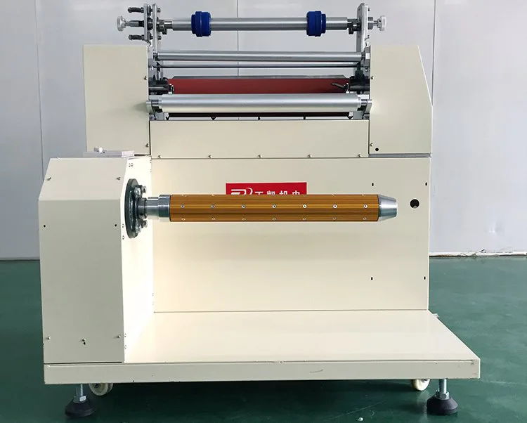
Flexible pcb material cutting machine
Use this table as a starting window, not a fixed recipe. The correct values depend on panel size, tool condition and edge target.
| Base film thickness | Adhesive system | Copper thickness | Suggested cutting window |
|---|---|---|---|
| 12–25 µm | Acrylic, epoxy or adhesiveless | 9–18 µm | Laser: 6–12 W, 100–300 mm/s, multi-pass; routing: 40k–60k rpm, feed 2–4 mm/s; shear only with sharp blade and low clearance |
| 25–50 µm | Acrylic or epoxy | 18–35 µm | Laser: 8–15 W, 80–250 mm/s; routing: 35k–50k rpm, feed 3–6 mm/s; shear clearance ≤5% of stack thickness |
| 50–75 µm | Epoxy or high-Tg adhesive | 35–70 µm | Routing preferred: 30k–45k rpm, feed 4–8 mm/s; laser with edge char check; shear for simple outlines only |
| 75–125 µm | Rigid-flex adhesive system | 35–105 µm | Routing or die punching; laser for openings only; verify depth control and burr limit |
Parameter ranges are process windows to validate on coupons. They are not a substitute for first-article inspection. For thin adhesive-heavy stacks, use lower stress methods and check for adhesive smear. For thick stacks, control tool wear and heat at the cut line.
This table closes a common gap: the same cut parameter cannot be copied from a thin two-layer stack to a thicker rigid-flex stack. Match base film, adhesive and copper before setting speed and depth.
Stackup Example: Cut Depth and Layer Relationship
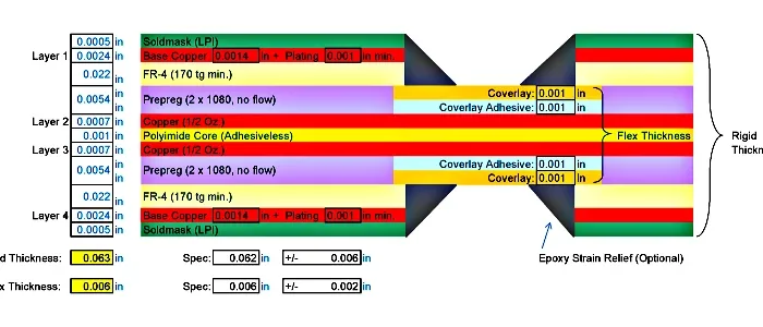
Use a cross-section sketch in the work instruction so operators can see where the cut should stop. A typical flexible stack looks like this:
“`
Top coverlay PI 25 µm
Coverlay adhesive 25 µm
Copper trace 18 µm
Adhesive 20 µm
Base PI 25 µm
Release liner / carrier 50 µm
—————————— controlled cut plane
“`
For panel singulation, cut through the full stack and stop in the carrier with 0.02–0.05 mm overcut. For access windows or coverlay openings, stop at the target layer and leave at least 0.05–0.10 mm clearance above the copper. If the drawing shows a partial-depth route, mark the safety margin and the inspection point on the same sketch. This prevents two common errors: cutting too deep into conductors and cutting too shallow so the panel tears during separation.
Flex PCB Cutting Cleaning and Edge Quality Control
Cleaning is not a cosmetic step. Residues block adhesion and cause plating defects.
Common methods are solvent wash, alkaline wash, ultrasonic cleaning and DI rinse. For high-reliability boards, plasma cleaning raises surface energy before lamination.
Edge quality is judged on four points.
- Burr and stringing. Loose material that folds over and bridges traces.
- Micro-cracks. Hairline fractures that grow during bending.
- Charring. Dark, carbonised edges after laser cutting.
- Contamination. Oils, dust and handling marks.
Check edges under magnification and log the result. A simple tape-lift check catches loose particles before lamination.
Inspection, Tolerances and Downstream Impact
Preparation quality shows up far downstream.
- Coverlay alignment. Clean, square edges give the coverlay a reliable datum.
- Adhesive squeeze-out. Consistent panel size controls overflow during lamination.
- Stiffener placement. Accurate fiducials keep stiffeners inside their zones.
- Panel utilisation. Better nesting raises yield per square metre.
State tolerances in one unit system. Mixing mil and mm on the same drawing invites errors. Also mark which dimension is critical and which is reference only.
Common Cutting Problems and Fixes
| Problem | Likely cause | Fix |
|---|---|---|
| Delamination at the edge | Dull blade or excess shear stress | Sharpen tooling; switch to routing or laser |
| Uneven or oxidised edge | Worn die or long storage | Trim before use; control storage humidity |
| Loose fibres and burrs | Incorrect feed or speed | Re-check parameters; add a deburr step |
| Size drift between lots | Temperature or humidity swing | Condition material before cutting |
| Weak adhesion after cleaning | Residual oils | Add DI rinse and plasma treatment |
Running this table as a shift checklist stops repeat defects. It also shortens the feedback loop between cutting and lamination.
Flexible PCBs share this workflow across single-sided, double-sided and multilayer builds. As a Flexible PCB Manufacturer, we keep the same criteria for every panel size. Detailed spec questions are answered in the PCB Manufacturing FAQ.
FAQ
What does flexible PCB material preparation include?
It includes incoming inspection, drying, cutting to panel size, fiducial marking, edge trimming and beveling, surface cleaning, and final inspection with controlled storage.
How do I choose a cutting method for polyimide flex material?
Match the method to volume, shape, stack and tolerance. Shearing suits simple panels; CNC routing suits medium complexity; laser cutting suits tight tolerances and complex outlines; die punching suits high volume. Then confirm the parameter window with a coupon before release.
Should polyimide film be baked before cutting?
Yes, when moisture control is uncertain. Moisture trapped in polyimide turns to steam during lamination and can cause delamination. Bake according to the material datasheet, record time and temperature, and cut after the film returns to handling temperature.
What edge and cleanliness limits should be specified?
Set limits for burr height, loose stringing, char zone, particle size and surface energy. A typical starting point is burr ≤50 µm, loose stringing ≤0.10 mm, char zone ≤0.10 mm, no visible particles >50 µm at 10x, and surface energy ≥38 mN/m before lamination when plasma cleaning is used.
Project Consultation for Cutting and Material Preparation
Send your stackup, base film thickness, adhesive system, copper thickness, panel size, annual volume and edge/cleanliness targets. We will return a practical material-preparation route: cutting method, parameter window, cleaning sequence, inspection criteria and storage controls. This is a process review for your panel, not a generic quote.
Related Posts
- Flexible PCB Material Stack-Up: Types & Performance — Related article
- Flexible PCBs Material Guide — Related article
- Flexible PCB: Features, Design Guide & Applications — Related article
- AI-Driven Optimization of Flexible Circuit Boards Production — Related article
- Cleaning PCB Boards — Related article