
Flexible PCB Material Stack-Up: Types, Functions, and Performance

Flexible PCB Material Stack-Up: Types, Functions, and Performance
Therefore, a Flexible PCB Material Stack-Up is the ordered set of layers that builds a flex circuit: a flexible insulating substrate, a metal foil conductor, an adhesive layer where needed, and a cover film. Additionally, each layer sets part of the bending, electrical, and thermal behavior of the finished board.
Stack-Up Layers at a Glance
Meanwhile, flexible PCBs start with four material groups. For example, the substrate carries and insulates the circuit. In addition, the metal foil forms the conductors. However, the adhesive bonds layers together. As a result, the cover film protects the outer circuit.

Basic Structure of FPCB
- Substrate: a flexible polymer film that carries the circuit and provides insulation.
- Metal foil: the conductive layer, normally copper foil, patterned by etching.
- Adhesive: the bonding medium between substrate and foil, and between other layers.
- Cover film: the surface protective layer, usually the same polymer type as the substrate.
- Stiffeners: local reinforcement added where the design needs a rigid area.
In practice, most production today begins with flexible copper clad laminate (FCCL). Next, it joins substrate, adhesive, and metal foil by lamination, so stack-up planning starts there.
FPC vs FFC: A Short Terminology Note
Consequently, a flexible printed circuit (FPC) is an etched copper pattern on a polymer film, and it is the subject of this page. Moreover, a flexible flat cable (FFC) is a straight conductor ribbon with extruded insulation and no etched circuitry. In particular, an FFC has no laminated stack-up to design, so material and layer planning as described here applies to the FPC.
FCCL: The Starting Point of Most Stack-Ups
However, FCCL is the primary raw material for flexible circuit boards. Therefore, it comes in two builds. Additionally, the three-layer type contains substrate, adhesive, and metal foil, and is called adhesive-bonded FCCL. Meanwhile, the two-layer type has no adhesive between substrate and foil, and is called adhesive-free FCCL.

Flexible Copper Clad Laminate (FCCL)

Performance Data of Flexible Substrates
For example, because there is no adhesive layer, the substrate keeps its own properties. In addition, that gives a thinner, lighter, and more flexible base. However, the bond strength between copper foil and substrate is relatively weaker. Adhesive-free FCCL is therefore selected for high-performance builds, such as High-Reliability Flexible Circuits for High-End Applications.

As a result, lamination is the common way to make adhesive-free FCCL. In practice, composite PI resin is coated or cast onto the roughened copper foil surface and the polyimide (PI) substrate. Next, the two are then stacked and hot-pressed. Consequently, a sputtering route is also used: metal ions form a conductive layer on the film, or a conductive metal layer is deposited by chemical plating. Moreover, sputtering can produce extremely thin conductive layers.
Core Layers: Substrate, Metal Foil, Cover Film, and Stiffeners

Substrates

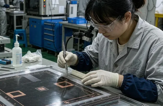
In particular, the substrate is a flexible polymer film. However, it loads the circuit and isolates it. Therefore, as the base layer, it defines the primary performance of the flexible circuit. Additionally, cutting and cleaning come before lamination, so flexible PCB material preparation already shapes final layer quality.
Metal Foil
Meanwhile, the metal foil is the conductive element, typically copper foil. Circuit patterns are formed by etching this foil. In a two-layer FCCL, the foil bonds to the substrate directly. In a three-layer build, the adhesive sits in between.
Cover Film
The cover film is the surface protective layer. It is usually a polymer film of the same type as the substrate, which keeps performance consistent across the board. Adhesive still bonds the cover film to the circuit layer. The same adhesive also joins multi-layer flexible circuits.
Stiffeners
Some stack-ups add a stiffener where the board must stay rigid, such as a connector area. Stiffener position and layer order are planned together, not added after routing.
Material Options Compared Across the Whole Stack
Stack-up decisions are rarely about one material. The table below places the usual options side by side so substrate, foil, bond, surface, and shielding choices can be weighed on the same page.
| Material choice | Stack function | What it contributes | Where it fits | Trade-off |
|---|---|---|---|---|
| PI (polyimide) substrate | Base dielectric and carrier | High heat resistance, dimensional stability, wide service temperature | Dynamic bend zones, reflow-exposed assemblies | Higher material cost than PET |
| PET (polyester) substrate | Base dielectric and carrier | Low cost, good general dielectric behavior | Static bend, low-temperature, cost-driven products | Lower heat resistance, limited soldering tolerance |
| Rolled copper foil | Conductor | Fine grain structure, high elongation, best fatigue life | Dynamic flexing zones and high-cycle bends | Fewer thickness options, higher price |
| Electrodeposited (ED) copper foil | Conductor | Broad thickness range, good fine-line etch, lower cost | Static bend areas and rigid sections | Lower elongation, cracks earlier under repeated bending |
| Adhesive-bonded (3-layer) FCCL | Base laminate | Strong peel strength, mature and predictable process | Standard flex and general multilayer builds | Thicker stack, lower flexibility, adhesive alters dielectric behavior |
| Adhesive-free (2-layer) FCCL | Base laminate | Thinner and more flexible, uniform dielectric thickness | Thin high-performance and dynamic builds | Lower foil-to-substrate peel strength, higher material cost |
| Coverlay (cover film plus adhesive) | Surface protection | Mechanical robustness, thicker protection, forgiving over large openings | General flex, connector and edge areas | Added thickness, adhesive flow, needs routed openings |
| Flexible solder mask (photoimageable) | Surface protection | Thin, fine opening geometry, low profile | Dense pad arrays, thin dynamic zones | Less mechanical protection, tighter process control |
| Shielding film or shield layer | EMI control and ground reference | Reduced emission, defined return path | High-frequency or noise-sensitive circuits | Adds thickness and stiffness, complicates bending |
Adhesive vs Adhesiveless: Which Build to Choose
The choice is a trade-off between compactness and bond strength.

Mucous Membrane

Properties of Selected Common Adhesives
| Build | Layers | Strength | Typical use |
|---|---|---|---|
| Adhesive-bonded FCCL | Substrate, adhesive, foil | Stronger bonding through the adhesive | Standard flex builds |
| Adhesive-free FCCL | Substrate and foil | Thinner and more flexible, weaker foil-to-substrate bond | High-performance flex builds |
Adhesive is still needed for cover film bonding and for joining multilayer flex circuits. Therefore, “adhesiveless” describes the base laminate, not the whole board. In practice, the adhesive decision is made first, because it sets the base thickness that every later layer must balance around.
Coverlay vs Flexible Solder Mask
Both protect the outer copper, but they behave differently in the bend zone.
| Aspect | Coverlay | Flexible solder mask |
|---|---|---|
| Build | Polymer film plus adhesive, laminated and cured | Photoimageable liquid, printed and developed |
| Thickness | Higher, adds a distinct layer | Low profile, thin over traces |
| Opening geometry | Routed or punched, limited by tooling | Fine openings defined by exposure |
| Mechanical protection | Good, resists abrasion and connector insertion | Moderate, thinner protection |
| Effect on bending | Stiffer in the covered zone | Better for thin dynamic zones |
| Process control | Adhesive flow and registration to manage | Cure and development control to manage |
A common approach is to use coverlay where the board meets connectors and edges, and flexible solder mask in dense pad fields or thin bending areas. Mixing the two on one board is acceptable when the transition is placed away from the bend line.
Shielding and Ground Layers in the Stack
When EMI or a controlled return path matters, the stack gains one or more of these options: a laminated shielding film bonded over the coverlay, a sputtered shield, or a dedicated copper ground layer inside a multilayer build. Each adds thickness to the bend zone, so shielded sections are usually kept out of the highest-cycle bending areas, and any ground layer is made solid rather than hatched where impedance control is required.
FPC Stack-Up Types and Their Trade-Offs
FPC stack-up types follow the number of conductor layers and the way they are bonded. Most Flexible Circuits use one of four builds.
| Type | Build | Function | Trade-off |
|---|---|---|---|
| Single-sided | One foil layer plus cover film | Simple routing and easy bending | Lowest routing density |
| Double-sided | Two conductor layers, adhesive or adhesiveless bond | More routing in the same outline | More process steps |
| Multilayer flex | Several circuit layers joined with adhesive | High routing density in a thin package | Stiffer bend zone |
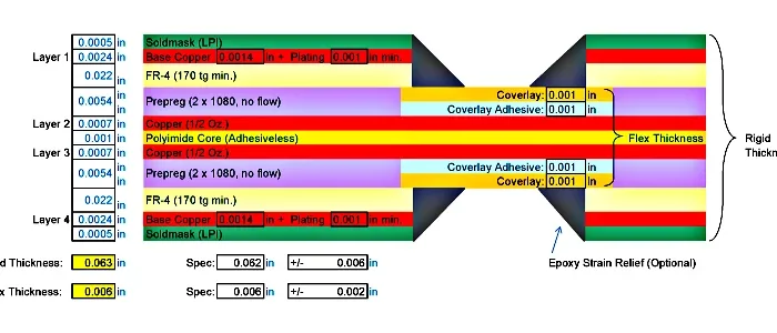
| Rigid-flex | Flex layers plus rigid sections in one board | Moving part and component area together | Longer build planning |
For repeated bending, a thin adhesiveless base is often the better starting point. For dense routing, multilayer builds add conductor layers, and each adhesive layer adds thickness. The fastest way to decide is to fix the bend requirement first, then choose the layer count.
Typical Stack-Up Examples by Layer Count
The layer sequence below is the working reference for quoting and DFM review. Read each line from the outer surface inward.
- Single-sided (1 conductor layer): coverlay or solder mask/copper foil / PI substrate / optional stiffener.
- Double-sided (2 conductor layers): coverlay / adhesive / copper / PI core (adhesive or adhesiveless bond) / copper / adhesive / coverlay.
- Multilayer flex (commonly 4 to 12 layers, extending to 18 layers in high-density designs): coverlay / adhesive/copper/bond ply / PI core/copper/bond ply / inner PI cores with copper / coverlay, with bond plies between each circuit layer.
- Rigid-flex: flex core of 2 to 6 conductor layers laminated between rigid sections that typically carry 4 to 18 layers in total, joined by no-flow or low-flow bond ply.
Layer counts above 12 are usually driven by routing density rather than by bending needs, and they are planned with the bend zone kept to the thinnest possible subset of layers.
Layer Count and Thickness Recommendation Matrix
Use the matrix as a starting point, then confirm with bend testing on the actual build.
| Bend profile | Recommended conductor layers | Base film thickness | Copper type and thickness | Relative cost | Yield sensitivity |
|---|---|---|---|---|---|
| Static bend during assembly only | 1 to 2 | 25 to 50 µm | ED copper, 18 to 35 µm | Low | Low |
| Occasional manual flexing | 1 to 2 | 25 µm | Rolled copper, 18 µm | Low to medium | Low |
| Continuous dynamic bending, moderate cycle count | 2 | 12.5 to 25 µm | Rolled copper, 12 to 18 µm | Medium | Medium, driven by coverlay registration |
| High-cycle dynamic bending | 1 to 2, thin build only | 12.5 µm | Rolled copper, 12 µm | Medium to high | High, sensitive to adhesive thickness variation |
| Dense routing with limited bending | 4 to 12 | 25 µm per core | ED or rolled copper, 12 to 18 µm | High | Medium to high, driven by lamination cycles |
| Rigid-flex with components on rigid sections | 2 to 6 flex layers plus rigid build | 25 µm per core | Matched foil types across the build | Highest | High, driven by bond ply flow and registration |
Two cost effects repeat across these rows. First, every additional lamination cycle lowers yield and lengthens lead time, so multilayer and rigid-flex builds carry a real cost step rather than a linear increase. Second, moving to thinner rolled copper and adhesiveless laminate raises material cost but can reduce total cost in dynamic applications, because fewer field failures and less rework offset the material premium.
Flex PCB Material Stackup Performance: What to Compare
Flex PCB material stackup performance depends on how the layers act together, not on one material alone. A Flexible PCB is only as good as the balance between base film, foil, adhesive, and cover layer.
| Parameter | Layer involved | Why it matters |
|---|---|---|
| Dielectric constant and loss factor | Substrate, adhesive | Signal behavior at high frequency |
| CTE | Substrate, foil | Dimensional stability through thermal cycles |
| Moisture absorption | Substrate, cover film | Process control and long-term reliability |
| Temperature rating | All layers | Soldering and reflow exposure |
| Bond strength | Adhesive or direct foil bond | Peel resistance after bending |
| Foil type and thickness | Metal foil | Bend fatigue in the flex zone |
Ask every supplier for the same parameter set, so the comparison stays fair. A datasheet value alone is not enough. The value must match the build you plan to laminate.
Dynamic Bend Life: How It Is Tested
Bend life is not a datasheet number; it is a measured result for a specific stack. The usual methods are a cyclic bend fixture that strokes the sample around a fixed mandrel, a repeated folding test, and a torsion or sliding-bend variant that mimics the actual product motion. In each case the sample is energized and the test runs until a failure criterion is met, typically a defined resistance rise or an open circuit.
What matters when you compare results:
- The mandrel radius and stroke must be stated, because life falls sharply as radius decreases.
- The failure criterion must be stated, since a 10% resistance rise and an open circuit give very different numbers.
- The tested coupon should mirror the production stack — same foil type, thickness, coverlay, and stiffener layout.
Bend Radius vs Copper Foil Type and Thickness
Two rules hold across most materials. Thinner copper survives more cycles than thicker copper of the same type, and rolled copper survives more cycles than electrodeposited copper at the same thickness. Bend radius then scales the result: common starting guidance is a static bend radius of roughly 6 to 10 times the finished stack thickness and a dynamic radius of 20 times or more, verified by test rather than assumed.
Because the neutral axis sits inside the stack, placing the copper layer near the middle of the build reduces the strain it sees. That is why a thin symmetric double-sided build can outlast a thicker single-sided build in a high-cycle zone.
Impedance Consistency Across the Stack
Controlled impedance depends on line width, dielectric thickness, dielectric constant, and the distance to a continuous reference layer. Adhesiveless laminate helps because the dielectric thickness is defined by the film alone rather than by film plus a variable adhesive layer. Two practices protect consistency further: keep the reference plane continuous through the bend region, and account for coverlay or solder mask thickness in the impedance model instead of treating it as negligible.
DFM and Manufacturability Checks Before Release
Four checks catch most stack-up errors before tooling starts.
1. Layer balance. Keep the build symmetrical around the neutral axis, so the board does not curl after lamination and cure.
2. Adhesive thickness. Extra adhesive gains bond strength, but it reduces flexibility and shifts dielectric spacing.
3. Cover film openings. Windows must match pad and connector areas, or the cover film lifts after assembly.
4. Stiffener and bend line. Keep stiffener edges out of the bending zone.
Static and Dynamic Bending in the Design
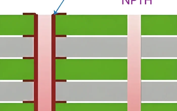
Define which areas bend once during assembly and which bend continuously in service. Static regions tolerate ED copper, thicker foil, coverlay, and added stiffeners. Dynamic regions should stay thin, use rolled copper, avoid plated through-holes entirely, and keep the bend line perpendicular to the traces rather than parallel.
Stiffener Zones and Outline Design
Place stiffeners under connectors, component pads, and test points, and stop them at least one stack thickness away from the bend line. On the outline, add relief where the flexible tongue meets the body of the board, avoid sharp internal corners, and keep the bend region free of coverlay openings and copper edges.
These checks apply to flexible circuit boards of every layer count. For material and process questions, the PCB Manufacturing FAQ covers the common points. Send the drawing and the bend requirement together, and a Flexible PCB Manufacturer can confirm layer order before tooling.
Bringing It Together: Material, Structure, Performance, and Cost
The same decision seen four ways, on one page.
| Stack decision | Structure effect | Performance effect | Cost and yield effect |
|---|---|---|---|
| PI vs PET substrate | Sets base thickness and layer count headroom | PI widens temperature range and improves dimensional stability | PI costs more per area but enables reflow and long life |
| Rolled vs ED copper | Same layer count, different fatigue behavior | Rolled copper extends dynamic bend life | Rolled copper costs more and narrows available thicknesses |
| Adhesive vs adhesiveless laminate | Removes one layer, thins the stack | Better flexibility and more uniform dielectric | Higher material cost, fewer process steps, less adhesive flow risk |
| Coverlay vs flexible solder mask | Changes outer layer thickness and openings | Coverlay protects mechanically; solder mask suits thin bend zones | Coverlay adds tooling and routing; solder mask adds process control |
| 1-2 layers vs 4-12 layers | Each layer adds a lamination cycle | Denser routing, stiffer bend zones | Yield falls and lead time rises with each cycle |
| Shielded vs unshielded | Adds a film or ground layer | Lower emission, defined return path | Thicker stack, stiffer bend, higher material cost |
FAQ
What are the main FPC stack-up types?
FPC stack-up types are grouped by conductor layers and bonding: single-sided, double-sided, multilayer flex, and rigid-flex. Each type can use adhesive-bonded or adhesive-free FCCL as its base, so one layer count may have two different builds.
Does adhesive-free FCCL always perform better?
Not always. Adhesive-free FCCL removes the adhesive layer, so substrate properties stay unaffected, and the base becomes thinner, lighter, and more flexible. However, the bond strength between copper foil and substrate is relatively weaker. It is chosen for high-performance FPCBs where thin, flexible builds matter.
Which layer defines flex PCB material stackup performance?
The substrate defines the primary performance of the flexible circuit, because it is the base layer. The metal foil, adhesive, and cover film then adjust electrical, mechanical, and protective behavior.
How is adhesive-free FCCL manufactured?
Two routes are common. In the laminating method, composite PI resin is coated or cast onto roughened copper foil and PI substrate, then hot-pressed. In the sputtering method, metal ions form a conductive layer on the film, or chemical plating deposits a conductive metal layer.
How many layers should a flexible PCB stack-up have?
Start from the bend requirement. Single-sided or double-sided builds cover most bending applications. Multilayer flex is chosen when routing density cannot be met in two layers; 4 to 12 layers is the common working range, and designs extend to 18 layers when required. Each extra layer adds a lamination cycle, so it should be justified by routing, shielding, or impedance needs rather than by habit.
What determines bend life in a flex stack-up?
Bend life is set mainly by copper type and thickness, bend radius, and the position of the copper relative to the neutral axis. Rolled copper and thinner foil last longer, a larger radius lasts longer, and a symmetric build keeps strain lower. Because these factors interact, life should be confirmed by a cyclic bend test on a coupon that matches the production stack.
How thick should each layer be?
Common substrate films are 12.5, 25, and 50 µm, with 25 µm the usual default. Copper is typically 12 to 35 µm, and thinner foil is preferred in dynamic zones. Coverlay adds roughly 25 to 50 µm, including adhesive. Keep the total bend-zone thickness as low as the routing allows, then check that the chosen radii meet the 6 to 10 times thickness guide for static bends and 20 times or more for dynamic bends.
Related Posts
- Flexible PCB Material Preparation: Cutting and Cleaning Process — Related article
- Flexible PCBs Material Guide — Related article
- Flexible PCB: Features, Design Guide & Applications — Related article
- AI-Driven Optimization of Flexible Circuit Boards Production — Related article