
Laser Solder Ball Bonding for FPCB: Low HAZ Protection

Laser Solder Ball Bonding for FPCB: Low HAZ Protection
Laser solder ball bonding for FPCB joins fine pads with a focused beam instead of bulk heat. However, the beam heats a metal ball, and conduction carries energy into the solder paste. Therefore, this keeps a low heat-affected zone FPCB process under 50 µm, limits substrate rise to ≤30°C, and holds delamination below 0.1%.

Laser Solder Ball Welding Machine
Why FPCB Substrates Fail Under Conventional Soldering Heat
Additionally, polyimide and PET films form the base of most flexible boards. Meanwhile, their heat resistance sits at or below 150°C. For example, copper traces are thin as well, mostly 12–35 µm. In addition, together, these two limits leave almost no thermal margin for any soldering step.
As a result, traditional iron soldering breaks that margin. In practice, the tip touches the board, so heat spreads by conduction across a 300–500 µm zone. Next, PI film then shrinks by more than 5%. Consequently, trace spacing narrows, and short circuits become likely.
Moreover, hot-air soldering is gentler in pressure but not in heat. Its heat-affected zone still reaches 200 µm or more. In particular, stream temperature swings of ±15°C mean a 180°C setting can spike past 200°C at local hot spots.
Therefore, the cover film and the adhesive under the copper take the damage first. However, delamination above 10% is common with iron contact. Therefore, measured defect rates for conventional FPCB soldering run 8%–12%.
How Laser Solder Ball Bonding for FPCB Delivers Heat
Additionally, laser solder ball bonding for FPCB reverses the heat path. Meanwhile, the beam never lands on the polymer. Instead, it heats a metal ball sitting on the pad, and conduction moves that energy into the solder paste.

Solder Ball
For example, published work on FPCB laser bonding describes the same chain. In addition, the laser heats a metal interconnector, and heat then transfers by conduction to the paste. As a result, energy arrives where the joint forms, not across the whole board.
In practice, because heating is local, the substrate stays cool. Next, substrate rise stays at or below 30°C, and the HAZ stays under 50 µm. Consequently, that is no more than a quarter of the hot-air figure.
Moreover, joint quality also depends on how time and pressure interact with temperature. In particular, if your line combines bonding with pressure, the laser welding FPCB guide covers those effects in detail.
Low Heat-Affected Zone FPCB Control: Three Process Innovations
However, a low heat-affected zone FPCB result comes from three linked controls, not from one setting on the machine.
Laser source optimization
Therefore, source choice sets the energy density ceiling. A stable beam profile keeps the spot round and its edges sharp, so the heated area matches the pad. Uniform spots avoid the hot rim that quietly widens the zone.
Closed-loop energy control
Power drifts as lenses warm and surface reflectivity changes. A closed loop samples each joint and corrects pulse energy in real time. As a result, every ball receives the same dose, and joint-to-joint variation stays small.
Non-contact bonding
No tip touches the pad, so no mechanical pressure lands on a 12–35 µm foil. In addition, there is no tool wear and no pad scrubbing. Ball placement and energy delivery stay fully independent.
Laser Soldering FPCB HAZ: Iron, Hot Air, Laser Compared
Comparing laser soldering FPCB HAZ data with legacy methods makes the gap visible. The table below uses process figures and separates local-heat methods from panel-heat methods.
| Method | Heat input | Cycle time | Typical HAZ | Yield indicator |
|---|---|---|---|---|
| Iron soldering | Contact conduction; 20–40 W tip | 2–5 s per joint plus cool-down | 300–500 µm | 8%–12% defect; yield 88%–92% |
| Hot-air soldering | Convection; 250–350°C stream | Seconds per joint or region; stream stabilization | ≥200 µm | 8%–12% defect; yield 88%–92% |
| Hot-bar / thermode bonding | Pulsed contact; pressure plus heat | 1–3 s per bond; tool dwell | 100–250 µm | 2%–5% defect; yield 95%–98%, planarity sensitive |
| Whole-board reflow | Panel-level convection or IR; 3–6 min profile | Minutes per panel; full ramp and cool | Board-wide thermal exposure | Warpage-driven defects; thin PI yield often below 95% |
| Laser solder ball bonding | Local conduction through the ball; ms pulse | <1 s per joint; no bulk cool-down | <50 µm | >99.6% at 0.15 mm joints |
Cycle time differs as well. Iron and hot air heat a region and then wait for the region to cool. Laser bonding heats only the joint, so the panel can move on at once. Hot-bar bonding is faster than iron, but the tool still contacts the joint and transfers heat through the tool. Whole-board reflow heats the entire panel, so warpage and CTE mismatch act on every joint at once.
HAZ Quantification: Temperature Gradient, Width, and Substrate Thresholds
A low-HAZ claim is only useful when it is measured. The process window should be defined by four quantities: the temperature gradient at the joint boundary, the HAZ width, the substrate warpage limit, and the delamination threshold.
| Metric | Target or limit | Verification method |
|---|---|---|
| Peak substrate temperature rise | ≤30°C | IR camera or fine thermocouple |
| HAZ width | ≤50 µm; ≤30 µm for 0.15 mm fine-pitch joints | Cross-section at 10× |
| Lateral temperature gradient | ≥100°C/mm at the ball edge; <20°C/mm at the HAZ boundary | Thermal simulation or IR line scan |
| Warpage | ≤0.1 mm over 100 mm; ≤0.2% of panel diagonal | Shadow moiré or laser scan |
| Delamination | <0.1% area; no visible delamination | C-SAM and cross-section |
The gradient matters because the polymer does not respond to peak power alone. Energy must fall from melting temperature at the ball to below the film transition range within tens of microns. If the gradient flattens, the HAZ widens even when the peak power is unchanged. A steep gradient also protects the pad edge, where the copper is thin and the coverlay adhesive is closest to the heat.
Warpage and delamination are the two substrate thresholds to lock first. A panel that passes shear but bows after bonding will fail at assembly. A joint that looks bright but shows a white edge under cross-section has already begun to delaminate.
Laser Parameter Window and Joint Quality
Four parameters define the working window: power density, pulse duration, spot diameter, and ball diameter. Each one pushes the joint in a different direction.
- Power density sets the melting rate. Too low leaves a cold joint with weak wetting. Too high drives voids and ball offset.
- Pulse duration controls how far heat conducts past the ball. Short pulses finish the joint before the polymer warms.
- Spot diameter should match or slightly cover the ball. An oversized spot spills energy onto bare PI film.
- Ball diameter sets the joint scale. The 0.15 mm joint is the reference case behind the yield data here.
When HAZ widens, cut pulse energy before you shorten the pulse. Shorter pulses with the same energy simply raise peak power and can damage the pad edge.
Material and Finish Selection: Lead-Free Balls, ENIG/OSP Pads, Flux Paths
Material selection fixes the wetting system before the laser parameters are set. For FPCB work, the usual choice is a lead-free solder ball matched to a pad finish that stays flat at fine pitch.
| Choice | Preferred options | Process note |
|---|---|---|
| Solder ball | Lead-free SAC305 or SnAgCu; low-temperature SnBi for PET | Match ball diameter to pad opening; confirm wetting within one pulse |
| Pad finish | ENIG for fine pads; OSP for cost-sensitive boards | ENIG flatness supports 0.15 mm joints; OSP needs active flux or tight oxide control |
| Flux path | No-clean or water-soluble flux; fluxless with inert gas | Flux improves wetting; fluxless needs clean pads, low oxygen, and a verified profile |
ENIG pads give a flat surface and predictable wetting, which helps when the ball is 0.15 mm or smaller. OSP is lower cost, but the oxide barrier must be removed by flux or by a fluxless path with good atmosphere control. For either finish, confirm shelf life and handling before bonding.
The flux decision changes the downstream process. No-clean flux leaves residue that must be compatible with the coverlay and test probes. Water-soluble flux needs a cleaning step that will not swell the PI or trap moisture. A fluxless path removes chemistry from the line, but it requires clean pads, low oxygen at the joint, and a parameter window that wets the ball before the surface re-oxidizes.
Material and Design Rules That Protect the Substrate
Material choice sets the limit; layout decides how close you run to it. PI film tolerates more heat than PET, so PET boards need the tighter window. Copper thickness matters too, since a 35 µm foil spreads heat faster than a 12 µm foil and shifts FPCB heat dissipation at the joint.
Keep the pad opening close to the ball diameter. A wide opening exposes more polymer and removes the metal path that shields the film. Also add a copper island or thermal relief under the pad so energy spreads sideways instead of downward.
Treat the coverlay as a thermal element too, because coverlay bonding strength drops once the adhesive passes its transition range. The same rule applies to wearable flex circuits, where a thin film sits close to heat-generating parts.
Process Implementation Checklist Before Production
Use this checklist to move from a lab joint to a controlled line. Each item should be signed off with measured data, not visual acceptance alone.
- Verify pad finish shelf life and oxide state. OSP panels need a cleanliness check before the first bond.
- Match ball alloy, ball diameter, and pad opening. Run a wetting coupon before the first panel.
- Select the flux path. If fluxless, set the inert atmosphere and confirm that the pad remains oxide-free through the pulse.
- Run a DOE over power density, pulse duration, spot diameter, and ball diameter. Lock the window with shear and HAZ data.
- Complete a first-article cross-section for HAZ width, delamination, and warpage. Compare against the quantitative limits above.
- Set SPC on pulse energy, spot size, and shear strength. Revalidate after lens, nozzle, or ball-feeder service.
- Define panel support and handling. Avoid mechanical stress before and after bonding, especially on thin PET and fine-line PI.
Verifying a Low Heat-Affected Zone: Inspection Checklist
Verification should prove the zone, not just the joint. Five checks cover most cases:
1. Ball shear or push test, to confirm joint strength against the drawing limit.
2. X-ray, to catch voids and ball offset under the pad.
3. Cross-section, to measure real HAZ width and confirm no delamination.
4. Thermal simulation or IR measurement, to confirm peak substrate temperature and the lateral gradient.
5. Bend test after bonding, to confirm the flex still meets its bend requirement.
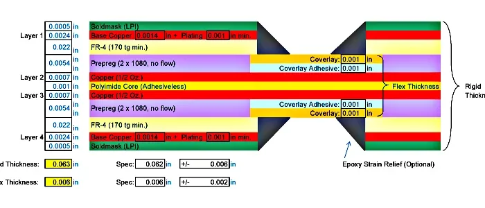
Medical and automotive builds, such as High-Reliability Flexible Circuits for High-End Applications, usually need all five. Multilayer and Rigid-Flex PCB Technology stacks need the cross-section step every time, because heat spreads differently across flexible circuit boards with more copper layers. For general substrate and finish questions, see our PCB Manufacturing FAQ.
FAQ
What is laser solder ball bonding for FPCB?
Laser solder ball bonding for FPCB is a non-contact joining method. A focused beam heats a metal ball on the pad, and conduction carries the energy into the solder paste. The polymer substrate is never directly heated, so the joint forms with a much smaller heat-affected zone than iron or hot-air soldering.
What HAZ can a low heat-affected zone FPCB process hold?
A low heat-affected zone FPCB process holds the HAZ under 50 µm and keeps substrate temperature rise at or below 30°C. Under those conditions, copper foil delamination stays below 0.1%, and yield exceeds 99.6% for 0.15 mm micro-solder joints. By comparison, iron soldering creates 300–500 µm zones, hot air at least 200 µm, hot-bar bonding about 100–250 µm, and whole-board reflow heats the entire panel.
What quantitative HAZ limits should be measured?
Measure four things: peak substrate temperature rise, HAZ width, lateral temperature gradient, and substrate warpage or delamination. A typical low-HAZ target is ≤30°C rise, HAZ ≤50 µm, lateral gradient ≥100°C/mm at the ball edge falling below 20°C/mm at the HAZ boundary, warpage ≤0.1 mm over 100 mm, and delamination <0.1% area. Cross-section, IR, shadow moiré, and C-SAM are the usual verification methods.
Why does laser soldering FPCB HAZ stay smaller than iron or hot air?
Laser soldering FPCB HAZ stays small because energy is delivered locally and on demand. Iron soldering spreads heat through contact, and hot air heats a whole region, so both warm the polymer around the joint. A laser pulse ends before heat can travel far into the PI or PET film, which is why the zone stays under 50 µm.
How does laser bonding compare with hot-bar bonding and whole-board reflow?
Hot-bar bonding is faster than iron and uses a controlled tool, but it still applies contact heat and pressure, so its HAZ is typically 100–250 µm. Whole-board reflow heats the entire panel for minutes and exposes every joint to warpage and CTE mismatch. Laser solder ball bonding heats only the ball and pad, with HAZ under 50 µm and a per-joint cycle under one second.
Which solder ball, pad finish, and flux path should I select?
Use a lead-free solder ball that matches the pad finish and the film limit. SAC305 or SnAgCu is common for PI boards; low-temperature SnBi can suit PET. ENIG is preferred for fine pads because it is flat; OSP works for cost-sensitive boards if flux or a fluxless oxide-control path is in place. Choose no-clean or water-soluble flux when residue can be managed, and choose fluxless only with clean pads, low oxygen, and a verified wetting window.
How do you troubleshoot common defects in laser solder ball bonding for FPCB?
Start with the defect signature. Ball offset points to spot-to-pad misalignment, uneven wetting, or flux starvation; correct alignment and confirm pad finish. Voids usually come from peak power too high, pulse too long, or pad contamination; lower energy, shorten the pulse, and clean the pad. Cold joints or non-wetting point to low dose, OSP oxide, or insufficient flux; raise dose and verify flux or inert gas. Delamination means the HAZ is too wide or the panel is unsupported; cut pulse energy, shorten the pulse, and improve support. Solder splash comes from flux outgassing or an oversized spot; adjust the profile and spot diameter. Warpage after bonding calls for local heat control, better panel support, and a check that the process is not acting as a panel-level reflow.
Related Posts
- Laser Welding FPCB: Time, Pressure & Temperature Effects — Related article
- AI-Driven Optimization of Flexible Circuit Boards Production — Related article
- Boosting PCB and FPCB Heat Dissipation — Related article
- Coverlay Bonding Strength Optimization in Rigid-Flex PCB — Related article
- Dual-Laser Etching and Cleaning for FCCL Blind Vias — Related article