
Dual-Laser Etching and Cleaning for FCCL Blind Vias: Achieving High Pr
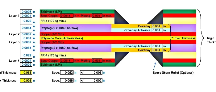
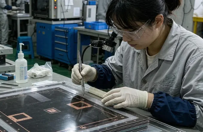

Flexible copper-clad laminate (FCCL), serving as the substrate material for flexible printed circuits (FPC), offers distinct advantages such as lightweight, flexibility, compact size, and excellent heat resistance.
Manufacturers widely adopt it in electronic products to achieve miniaturization and portability. This approach aligns with the development trends of high-precision electronics industries such as micro-robotics, new energy vehicles, 5G communication devices, and flexible displays.
However, traditional micro-hole processing methods—such as mechanical drilling, plasma hole formation, and electrochemical etching—have hindered the application and advancement of FPCs. These limitations stem from insufficient processing precision, low efficiency, high stress generation, and environmental pollution.
Advantages and Challenges of Laser Micro-Hole Processing
Laser micro-hole processing offers significant advantages, including universal applicability across materials, non-contact operation, high precision, low stress, and environmental friendliness. Consequently, it has seen widespread adoption in flexible circuit board manufacturing in recent years.
Current research efforts to enhance the precision and quality of micro-hole processing in flexible copper-clad laminates primarily focus on two approaches. One involves optimizing nanosecond laser processing parameters, while the other adopts ultrafast lasers, mainly femtosecond lasers.
Thermal effects, particularly excessive heat generation, inherently constrain the former approach and limit fundamental breakthroughs. The latter faces challenges such as high equipment costs and relatively low processing efficiency.
Concurrently, research on dual-laser combined etching and cleaning for FCCL remains scarce.
Blind Vias and Buried Vias in FCCL: Where Dual-Laser Etching Fits
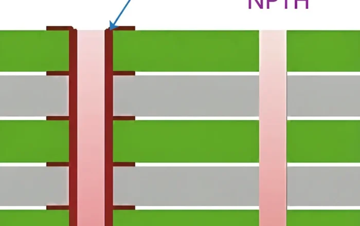
A blind via connects outer copper to a target pad without opening the full stack. A buried via connects inner layers and is not open to the outer surface. This page focuses on blind vias because the laser must stop on the bottom pad and then clean the same hole. The depth-control logic also helps when a buried via is opened after lamination, but the access layer and endpoint strategy change. Use this blind-via section as the transition to the material and parameter choices below.
Dual-Laser Etching and Cleaning for FCCL
Therefore, this study employs a dual-laser system to perform first-order blind via processing on FCCL using a layered etching method:
First, a UV nanosecond laser performs windowing on the copper layer using a concentric circular scanning method;
Subsequently, operators use both UV nanosecond and UV picosecond lasers to etch the polymer layer via a helical scanning method, simultaneously cleaning the entire blind hole;
Finally, researchers comprehensively compared and analyzed nanosecond and picosecond laser processing based on experimental data and acquired images. They evaluated etching depth precision, hole bottom and surface roughness, and overall morphology.
This simultaneously validated the processing quality of this dual-laser (etching and cleaning) process, achieving high-precision, high-quality, and high-cleanliness blind hole processing for FCCL.
Laser-Material Interaction Mechanisms
The interaction mechanism between ultraviolet lasers and FCCL involves photothermal removal and photochemical stripping.
Specifically, photothermal mechanisms dominate during metal etching. Under intense laser irradiation, intense bremsstrahlung causes free electrons in the skin layer to absorb energy, inducing electron thermalization.
At this stage, electrons exhibit a Fermi-Dirac distribution, and they transfer the absorbed photon energy to the crystal lattice via electron-phonon coupling, allowing the lattice to establish thermal equilibrium in approximately 100 ps.
Stages of Photothermal Interaction
Additionally, the photothermal mechanism exhibits four distinct stages at different power densities, as illustrated in Figure 1:
- Figure 1(a) depicts heat absorption in the skin layer.
- Fig. 1(b) depicts material melting and crater formation (where thermal wave propagation exceeds vaporization rates, accompanied by rising gas pressure, driving material penetration deeper).
- Figure. 1(c) illustrates evaporation jet formation;
- Fig. 1(d) shows vaporization jet perforation.

Figure 1: Four Stages of Laser Material Interaction at Different Power Densities
The dominant stage varies with different laser power densities. For instance, at power densities of 10⁸–10¹⁰ W/cm², the vaporization jet dominates material removal, significantly reducing thermal effects.
Photochemical Effects on Polymers
When ultraviolet lasers interact with polymers, both photothermal and photochemical stripping mechanisms occur simultaneously.
The single-photon energy of the emitted laser is 3.47 eV, exceeding the bond energies of C–C and C–N bonds in polyimide under normal conditions (approximately 3.4 eV). This enables direct cleavage of these chemical bonds, achieving relatively cold processing.
Ultrafast Laser Processing for Enhanced Precision
Overall, operators should minimize or avoid thermal effects to enhance processing quality. This means achieving material removal via vaporization while operating near the material’s damage threshold.
Since the pulse width’s relationship with the material’s electron-phonon relaxation time determines whether thermal effects occur during processing, it is essential to control the laser-material interaction time to ≤ 10⁻¹² s (picosecond scale), ensuring termination before energy transfer occurs between lattice sites (phonon-phonon relaxation).
Ultrafast lasers simultaneously satisfy the above conditions, delivering pulses with extremely high peak power at picosecond pulse widths that instantly reach the material’s damage threshold.
Furthermore, the pulse width of ultrafast lasers is shorter than the characteristic time of most physicochemical processes. At the same frequency, they offer a higher duty cycle, enabling longer cooling times that further suppress thermal effects.
Under these conditions, non-thermal processes dominate, significantly enhancing processing precision and quality.
Process Capability and Applicable Materials Comparison
Use this selection table to compare material response before fixing a recipe. The windows are starting points, not fixed settings.
| Material or layer | Role in FCCL blind via | Dual-laser response | Typical starting window | Main control point |
|---|---|---|---|---|
| FCCL copper foil | Window opening through outer copper | UV nanosecond removal with concentric scan | 355 nm class, 10-30 ns, 2-8 passes | Edge burr, window diameter, recast |
| FCCL polyimide | Main dielectric to be etched | Nanosecond roughing plus UV picosecond finishing | Low fluence finishing, 10-20 ps class | Depth per pass, taper, carbonization |
| Adhesive layer | Bond line between dielectric layers | Reduced-energy nanosecond and picosecond passes | Lower fluence, higher overlap | Smear, bleed and depth offset |
| Cover film | Outer protection after via formation | Opened only when design requires it | Lower energy, larger overlap | Registration and delamination |
| EMI shielding film | Shielding layer over flex | UV nanosecond for thin metal, picosecond for polymer | Multi-step, low thermal load | Shield damage and residue |
| PSA | Pressure-sensitive adhesive layer | Cold cleaning at low fluence | Low power, multiple light passes | Adhesive flow and residue |
This table is for horizontal selection. Confirm the final window with cross-sections on the actual FCCL stack.
Material-by-Material Process Windows: FCCL, Adhesive, Cover Film, EMI Shielding Film and PSA
FCCL copper and polyimide
Copper windowing sets the via diameter and the edge quality. Polyimide etching sets the depth. Run copper removal first, then switch to polymer removal with a lower energy per pass. Keep the helical overlap high enough to avoid ridges on the wall.
Adhesive layer
The adhesive layer is the most common source of wall smear. Use a thin adhesive or an adhesive-free FCCL where the design allows it. If adhesive is present, reduce pulse energy and add light cleaning passes. Do not judge depth from the first pass, because adhesive removal differs from polyimide removal.
Cover film
Cover film is not always opened in the same step as the blind via. When it is opened, register the cover film window to the via and keep energy below the level that causes delamination. A separate cover-film opening step is often cleaner than forcing one recipe through two different polymers.
EMI shielding film and PSA
EMI shielding film adds a thin metal layer and a polymer carrier. PSA adds a soft adhesive layer. Treat these as layered materials, not as one homogeneous surface. Open the thin metal with the UV nanosecond beam, then finish the polymer and PSA with low-fluence picosecond passes. This layered approach protects the shield and reduces adhesive residue.
FCCL Blind Via Laser Etching: Depth Control and Quality Metrics
FCCL blind via laser etching is judged on five points. These are etch depth precision, bottom pad integrity, hole taper, sidewall roughness and hole bottom roughness. Surface morphology across the panel is a sixth check.
Depth control starts with pass count. Each helical pass removes a fixed increment of polymer. So the operator sets the pass number against the target depth, then confirms it with cross-section images. Optical inspection covers taper and diameter. Roughness is read from the hole bottom and from the surface.
Key process parameter window
| Parameter | Typical starting window | Control note |
|---|---|---|
| UV nanosecond wavelength | 355 nm class | Copper absorption and window opening |
| Copper window scan | Concentric, 2-8 passes | Edge quality and diameter |
| Nanosecond pulse width | 10-30 ns | Bulk removal with controlled heat |
| Picosecond pulse width | 10-20 ps | Low thermal damage finishing |
| Helical overlap | 30-70% | Wall taper and residue |
| Depth increment per pass | 2-8 um polymer per pass | Confirm by cross-section on your stack |
| Focus offset | Within about 10-20 um of best focus | Taper and bottom roughness |
| Cleaning pass energy | Below pad-damage threshold | Residue removal without pad damage |
Defect, cause and countermeasure
| Defect | Likely cause | Countermeasure |
|---|---|---|
| Over-etch, pad damage | Too many passes or high pulse energy | Lower energy, add endpoint check |
| Carbonized PI residue | Long pulse, heavy thermal load | Add picosecond finishing passes |
| Adhesive smear at wall | Thick adhesive layer | Move to adhesive-free FCCL, re-focus |
| Large taper | Focus drift, low scan overlap | Correct focal offset, raise overlap |
| Loose debris in hole | Cleaning step skipped | Keep the in-line cleaning pass |
A UV picosecond laser FPC via cut leaves a narrower heat-affected zone. That helps when the target is a small via in thin polyimide.
Throughput, Yield and Cost: Dual-Laser vs Single-Laser Planning Data
Capacity, yield, and cost should be compared at the panel level, not by tool price alone. The table below gives indicative planning ranges for 50- 75 µm blind vias. Validate them against your via count, copper thickness, and design rules.
| Metric | Single nanosecond laser | Dual-laser etching and cleaning | Planning note |
|---|---|---|---|
| Relative throughput | 1.0x baseline | 1.3-1.8x | Higher when finishing and cleaning replace a separate step |
| First-pass yield in stable window | 92-96% | 96-99% | Requires endpoint checks and cleaning validation |
| Main scrap driver | Over-etch and residue | Lower over-etch, fewer cleaning defects | Inspect bottom pad and wall |
| Cost per panel | Lower capex | Higher capex, lower rework | Compare total cost, not purchase price |
| Best fit | Coarser vias, lower density | Dense, thin, high-reliability FCCL | Match capability to design rules |
The dual-laser scheme usually wins when the design has small vias, thin dielectric, and a high cost of rework. A single-laser scheme can still be the lower-cost choice for coarse features and loose depth tolerance.
Laser Etching/Cleaning vs Laser Marking/Cutting
Laser etching and cleaning remove dielectric to a controlled depth and stop on the target pad. Laser marking changes surface appearance for identification. Laser cutting severs the material through its thickness. These are different operations and should not share recipes.
| Operation | Purpose | Depth intent | Typical risk |
|---|---|---|---|
| Laser etching and cleaning | Open and clean a blind via | Controlled depth to pad | Over-etch, residue, taper |
| Laser marking | Surface ID or color change | Minimal material removal | Reading a mark as a depth result |
| Laser cutting | Sever outline or opening | Through-cut | Using cut settings for a blind via |
Do not transfer marking or cutting parameters to blind-via etching. The optics, pulse energy, and endpoint logic are different.
Laser-Material Interaction Mechanisms
UV laser interaction with FCCL combines photothermal removal and photochemical stripping. Photothermal action dominates during metal etching. Under strong irradiation, free electrons in the metal skin layer absorb energy, so heat builds fast at the surface and copper leaves as vapor and ejecta.
The polymer layer behaves differently. Here photochemical bond breaking competes with thermal ablation. A shorter pulse tips the balance toward clean stripping. That is why the picosecond beam cleans the wall as it finishes the hole.
Cleaning Verification: Residue, Carbonization and Adhesion
Etching leaves residue behind. Typical issues are carbonized polyimide, redeposited copper particles, and adhesive overflow at the rim. Left in place, they weaken the plated joint.
Therefore, the flow includes an in-line clean. Verification follows three checks: surface cleanliness under inspection, contact angle on the via bottom, and plating adhesion after seeding. The same discipline used to keep cleaning PCB Boards free of residue applies inside the hole. For plating reliability, a Carbon-Coated Film Evaluation is another useful reference point.
Experimental Design
This experiment utilized double-sided FCCL with a thickness of 49 μm as the test specimen, comprising:
- copper foil (Cu) with a thickness of 12 μm (primarily serving a conductive function);
- polyimide (PI) with a thickness of 25 μm (providing structural support);
- and first-order blind holes with a diameter of 120 μm and a depth of 37 μm processed in this study.
Table 1 lists the laser processing equipment parameters.

Table 1: Laser processing experimental equipment parameters
Researchers used LEXT OLS500 3D laser confocal microscopes for observation and acquired confocal images with a 1405 nm laser diode and a high-sensitivity photomultiplier tube, achieving a lateral resolution of 0.12 μm. Figure 2 shows the experimental scheme.

Figure 2: Experimental Setup
Laser Processing Methodology
In the first stage, operators used an ultraviolet nanosecond laser with a concentric circle scanning method. By adjusting the laser parameters, they etched a 120 μm diameter, 12 μm thick window onto the copper-clad laminate, completely removing the copper foil and exposing the polymer layer.
The second stage employed both nanosecond and picosecond lasers for polymer layer etching and cleaning, respectively. Researchers applied a spiral scanning method, treating laser power, frequency, scan count, and scan speed as the four factors, and conducted an orthogonal experimental design with four levels for each factor.
Parameter Optimization and Validation
Researchers used etching depth and surface roughness data to identify the influence weights and best levels for each factor, selected the optimal parameter combination through a comprehensive balancing method, and carried out validation and comparative experiments with this set.
Figure 3(c) illustrates the spiral scanning etching and cleaning process for the copper-clad laminate, with an inter-path spacing of 30 μm.

Figure 3 Schematic Diagram of FCCL First Order Blind Via Processing
To achieve thorough cleaning of surface overlayers, operators set the spiral top radius to 80 μm—extending 20 μm outward from the blind hole radius—thereby forming an annular cleaning zone around the micro-holes.
During the experiments, researchers used a metallurgical microscope and a laser confocal microscope for real-time rapid scanning and image acquisition of the blind holes. At the same time, they measured etching depth as well as surface and bottom roughness.
To more accurately reflect processing quality and error issues, each parameter set underwent 100 repeated trials, with surface roughness (rather than line roughness) serving as the evaluation criterion.
Analysis of Experimental Results
Analysis of Nanosecond Laser Window-Opening Test Results
Figure 4 presents laser windowing processing images. Figure 4(a) and (b) show observations under conditions of power P = 6 W, frequency f = 100 kHz, scanning speed v = 550 mm/s, and scanning count n = 2, captured using a metallurgical microscope and a laser confocal microscope, respectively.

Fig. 4: Cross-section of laser-etched copper layer
A window with a diameter D = 122.24 μm and a deviation value of 2.24 μm was obtained. The etching depth was approximately 14.28 μm, with minimal over-etching of the polymer layer, achieving complete removal of the copper layer.
As shown in Fig. 4(b), distinct spatter deposits and spurs were observed at the edges of the micro-holes, with a measured surface roughness of 2.13 μm.
Analysis of Orthogonal Test Results
◊ Analysis of Nanosecond Laser Orthogonal Test Results
Continuing etching after windowing, preliminary ranges for processing parameters in nanosecond laser etching of polymer layers were determined based on extensive experimental data.
An orthogonal test was designed with four factors—laser power (A), repetition rate (B), scan count (C), and scan speed (D)—each at four levels. Table 2 presents the factor level table.

Tab 2: Factor level table
An L16(44) orthogonal experiment was designed based on the factors and levels in Table 2. Table 3 presents the orthogonal experimental design and results.
Table 3 indicates that different combinations of processing parameters yield varying blind hole depths and roughness values. When analyzing data to identify the optimal processing combination, the weight assigned to processing depth in the evaluation criteria is greater than that assigned to roughness.

Tab 3 Orthogonal experimental factor design and results
» Range Analysis of Orthogonal Test Data
Table 4 presents the range analysis results of the orthogonal test data. The k value represents the mean etching depth and roughness corresponding to a given factor at different levels.
For etching depth, achieving the target depth takes priority. Within each factor, the closer the k value is to 37.00 μm, the more likely that level represents the optimal parameter for that factor under the etching depth criterion.
For example, in Table 4, under the etching depth factor, k2 is closer to 37.00 μm than k3 in the scan count levels. However, since the k2 level fails to meet the required etching depth, the k3 level should be selected as the optimal parameter for this factor.
Regarding roughness, a smaller k value under a given factor indicates that the corresponding level represents the optimal parameter for that factor in terms of roughness.
The Range (R value) represents the range of k values for a given factor, reflecting the influence of each factor on the test results (R value is proportional to correlation).
Table 4 indicates that the influence weights of factors on etching depth are A > C > B > D, with average power having the most significant impact.

Table 4 Range analysis
» Parameter Optimization and Comprehensive Balancing
Comparing the k values of each factor allows selecting the combination A2B2C3D2. The magnitude of influence on roughness is A > B > C > D, with average power having the most significant impact. Following the principle of selecting the smallest k value, one can choose the combination A2B4C2D3.
The comprehensive balancing method is applied to optimize the two selected parameter combinations:
1) Power. The optimal level factor for the first parameter in both sets is A2, thus selecting A2.
2) Repetition frequency. The optimal frequency levels in the two sets are B2 and B4. While B2 achieves complete polymer layer removal, it causes over-etching and yields the highest roughness. B4 produces the lowest roughness but suffers from insufficient etching depth. Therefore, B3 is selected.
Similarly, the study determines the optimized parameters for processing cycles and speed. Thus, the optimal parameter combination for the nanosecond laser in this process is A2B3C3D2, corresponding to: power P = 3.5 W, repetition frequency f = 100 kHz, processing cycles n = 3, and scanning speed V = 800 mm/s.
◊ Analysis of Picosecond Laser Orthogonal Test Results
A picosecond laser simultaneously etched the PI layer and cleaned blind vias, following evaluation metrics and principles consistent with Section 4.2.1.
Each of the four processing factors received four levels; the team designed orthogonal experiments and analyzed the data using the online statistical software SPSSAU. Table 5 presents the factor level table.

Table 5 Factor level table
Based on Table 5, an L16(4⁴) orthogonal experiment was designed for each factor and level. Table 6 presents the orthogonal experiment design and results.
Table 6 shows that etching depths fluctuated between 34.35 and 38.24 μm across different parameter combinations, with both incomplete etching and over-etching phenomena observed.

Tab 6. Orthogonal experimental factor design and results
The bottom surface roughness fluctuates between 0.23 and 0.75 μm, showing minimal overall variation. This indicates negligible or absent thermal effects during picosecond laser processing.
Table 7 indicates that for etching depth, the influence weights of each factor are A > B > C > D, with output power having the greatest impact.

Table 7 Range analysis
Based on the optimal levels of each factor, the parameter combination A3B1C4D1 is selected. Similarly, for surface roughness, the influence weights of factors are A > D > C > B. Based on the optimal levels, the selected parameter combination is A4B2C2D1.
After comprehensive balancing, the selected parameter combination is A3B1C4D1, corresponding to power P = 5 W, repetition rate f = 80 kHz, processing cycles n = 7, and scanning speed V = 800 mm/s.
Experimental Validation and Comparative Analysis
Based on the optimal parameter combinations selected for both nanosecond and picosecond lasers, copper-clad laminates were etched.
Table 8 shows that under optimized parameters, both lasers achieved significantly improved processing accuracy and quality. The picosecond laser demonstrated superior etch depth, hole bottom roughness, and surface roughness compared to the nanosecond laser.

Table 8. Optimization process etching results
◊ Hole Bottom Morphology
Bottom surface under nanosecond laser:
Figure 5(a) shows a darker bottom brightness with scattered black spots (unremoved polymer melt and copper-carbon mixture);
Figure 5(c) shows pronounced undulating patterns at the bottom. Compared with the picosecond laser, the longer exposure time of the nanosecond laser allows residual heat to diffuse into the surrounding area through thermal effects.
This diffusion increases undulations in the etched grooves and ultimately results in higher roughness and damage to the copper layer.
Picosecond laser-treated hole bottom:
Figure 5(b) exhibits high brightness (reflected light from the copper layer, indicative of cleanliness) and excellent uniformity, with virtually no dark spots or obstructions;
Figures 5(c), 6(b), and 6(d) demonstrate exceptionally high bottom flatness and cleanliness, with negligible protrusion. This achieves complete removal of polymers and residues while preserving the integrity of the substrate morphology.
◊ Surface Cleaning Zone:
As shown in Figure 5(a), a distinct annular cleaning zone exists at the microhole edges. Under nanosecond laser irradiation, both the cleaning range and etching scratches are larger than those under picosecond laser irradiation. Although the deposits are cleaned, damage is inflicted on the copper layer.
As shown in the blind hole surfaces of Fig. 5(b) and Fig. 6(a), the picosecond laser exhibits no significant ablation phenomena.
Surface spatter is effectively removed, and the etching marks are shallow, effectively preserving the morphology of the copper layer.
After laser cleaning, the surface roughness decreased from 2.13 μm to 0.25 μm, achieving significant improvement.

Figure 5. Observation of Blind Holes After Laser Etching and Cleaning
Sidewalls: Figures 6(b) and (d) display cross-sectional views of the blind hole. The images reveal excellent sidewall uniformity with no overhanging material, no significant resin shrinkage, and no serrated etching scratches.

Figure 6. Schematic of picosecond laser etching and cleaning of blind holes under optimized parameters
Conclusion
Dual-Laser etching and cleaning for FCCL Blind Vias links three steps: nanosecond copper windowing, mixed nanosecond and picosecond polymer etching, and in-line cleaning. Splitting roughing from finishing keeps depth error low and sidewalls clean. The same logic supports material-specific windows for FCCL, adhesive layers, cover film, EMI shielding film, and PSA. For denser flex builds, the same quality thinking appears in Rigid-Flex PCB Technology and in High-Reliability Flexible Circuits for High-End Applications. It also matters for wearable flex circuits, where thin substrates and small vias dominate. More process questions are answered in our PCB Manufacturing FAQ.
FAQ
What is FCCL blind via laser etching?
FCCL blind via laser etching is a laser-only method that cuts a via from the copper side down to the bottom pad of a flexible copper-clad laminate. A UV nanosecond laser opens the copper, then nanosecond and picosecond beams remove the polymer and clean the hole in one flow.
Why combine nanosecond and picosecond lasers?
The nanosecond beam removes copper and bulk polymer quickly, which keeps throughput up. The picosecond beam finishes the polymer with a short pulse, so less heat reaches the sidewall and the bottom pad. Together they balance speed against precision.
How do you stop over-etching and bottom pad damage?
Control the number of helical passes against the target depth, keep pulse energy low, and verify depth by cross-section before scaling up. A short picosecond finishing pass also limits thermal load at the bottom pad.
How is laser etching and cleaning different from laser marking or cutting?
Etching and cleaning remove dielectric to a controlled depth and stop on the pad. Marking changes the surface for identification, and cutting severs the material. Do not use marking or cutting recipes for blind-via depth control.
Which FCCL materials need separate process windows?
Treat FCCL copper and polyimide, adhesive layers, cover film, EMI shielding film, and PSA as separate material groups. Each group has a different absorption and thermal response, so set energy, overlap, and pass count per layer rather than using one blanket recipe.
What throughput, yield, and cost trade-off should be expected?
In planning terms, a dual-laser scheme can raise relative throughput and first-pass yield while reducing rework. It also carries higher capex than a single nanosecond laser. Compare total panel cost, defect rate, and design density before selecting the scheme.
Related Posts
- Optimizing Blind Slot Multilayer Flexible PCB Manufacturing — Related article
- Adhesive-Free FCCL Substrates vs Adhesive-Based FCCL — Related article
- Carbon-Coated Film Evaluation for Reliable FCCL Copper Plating — Related article
- Cleaning PCB Boards — Related article
- FCCL vs. Rigid Copper Clad Laminate: Key Differences — Related article