
PCB Drilling Techniques: Laser vs Mechanical, Hole Types & Quality Inspection

What is PCB Drilling and Why It’s Crucial
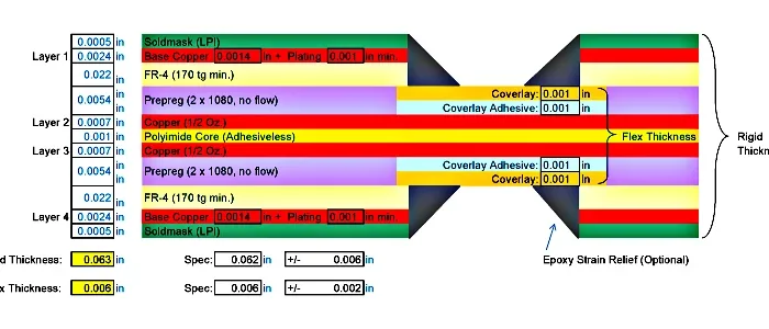
PCB drilling is the process of making holes in PCBs. This helps connect different layers electrically or hold components in place. It’s a key process in making multi-layer and rigid-flex PCBs. It allows signals and power to move up and down through stacked layers of copper.
Selecting the right drilling method ensures not only electrical continuity but also structural integrity and long-term performance.
PCB Drilling Techniques fall into two main families: mechanical CNC drilling for standard holes from 0.15 mm up, and laser drilling for microvias of 0.1 mm and below. Choosing between them shapes hole quality, yield, and cost. This guide compares both, explains hole types, and shows how to inspect flex PCB drilling quality.
Laser vs Mechanical Drilling: Side-by-Side Comparison
Most engineers ask one question first: which method fits the hole? The table below gives a head-to-head view of laser vs mechanical drilling across the factors that decide yield and cost.
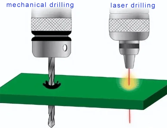
PCB mechanical drilling and laser drilling
| Factor | Mechanical (CNC) | Laser |
|---|---|---|
| Minimum hole size | 0.15 mm and above | 0.1 mm microvias and below |
| Contact | Drill bit touches the panel | No physical contact |
| Typical materials | Rigid FR4, PTH and standard vias | Thin dielectrics, HDI, flex circuits |
| Throughput | High for large panels and big holes | Thousands of holes per second |
| Capital cost | Lower equipment investment | Higher equipment investment |
| Best fit | Large-scale rigid production | Miniaturized, high-density designs |
Cost and Throughput Trade-Offs
Mechanical drilling wins on capital cost. However, bit wear adds tool replacement cost over long runs. Laser drilling needs a bigger investment upfront. In exchange, it removes contact stress and reaches very small diameters fast. Therefore, the cheaper method depends on hole count, diameter, and volume.
Choose Your Method: Matrix by Hole Size, Layer Count, and Volume
Use this matrix to pick the drilling route before release. It maps hole size, stack complexity, and order volume to the method that usually gives the best yield and cost balance.
| Hole size | Layer count/stack | Volume | Recommended method | Process note |
|---|---|---|---|---|
| 0.15 mm and above | 1–8 layers, rigid FR4 | High | Mechanical CNC | Fast and low capital; standard PTH workhorse |
| 0.15–0.3 mm | 8–16 layers, rigid | Medium | Mechanical CNC with tight parameters | Watch aspect ratio and bit wear |
| 0.1 mm and below (microvia) | HDI, sequential build | High | Laser (UV) | No contact; thousands of holes per second |
| 0.1 mm and below | Flex or rigid-flex, thin dielectric | Low–medium | Laser | Avoids mechanical stress on polyimide |
| Mixed: 0.15 mm+ and 0.1 mm− | Rigid-flex or HDI | Any | Both on same panel | Mechanical for PTH; laser for microvias |
| 0.15–0.2 mm | >16 layers, high aspect ratio | Low | Mechanical with pilot hole / step drill | Reduces wander and heat; review before release |
For borderline cases, confirm the shop’s proven aspect ratio and minimum via diameter. When volume is low and the hole is small, laser may still win because tool wear and breakage costs drop. When volume is high and holes are large, mechanical drilling usually stays cheaper.
What is PCB Drilling and Why It’s Crucial
PCB drilling is the process of making holes in PCBs. This helps connect different layers electrically or hold components in place. It’s a key process in making multi-layer and rigid-flex PCBs. It allows signals and power to move up and down through stacked layers of copper.
Selecting the right drilling method ensures not only electrical continuity but also structural integrity and long-term performance.
Mechanical Drilling: Parameters, Tooling and Limits
Mechanical drilling remains the industry workhorse. It uses carbide or diamond-coated drill bits in high-speed CNC machines. The method suits plated through holes, standard vias, and large-scale production.
Four settings drive quality: spindle speed, feed rate, hit count, and retract rate. For example, worn bits drift off position and raise hole wall roughness. In addition, heat builds up fast in multilayer stacks. That heat can cause delamination when feed and speed do not match the stack-up.
Chip evacuation matters too. Poor dust removal packs debris into the hole and blocks plating later. So operators balance retract speed against vacuum strength. For micro tools on thin substrates, these settings deserve extra care, as covered in Improve PCB Micro-Drill Performance on Flex Boards.
Laser Drilling: UV, CO₂ and Excimer Options
Laser drilling removes material with a focused beam instead of a bit. CO₂ sources cut dielectric layers efficiently. UV sources use shorter wavelengths for finer features, and excimer sources serve niche fine-pitch work.
Because there is no contact, mechanical stress disappears. This matters for HDI and flex designs. Laser drilling also supports microvias of 0.1 mm and below, which modern phones, wearables, and 5G modules rely on.
The trade-offs are clear. Equipment cost is higher, and the method is limited to thin dielectric layers. Therefore, laser shines in high-density builds rather than thick rigid boards.
Types of Holes in PCBs
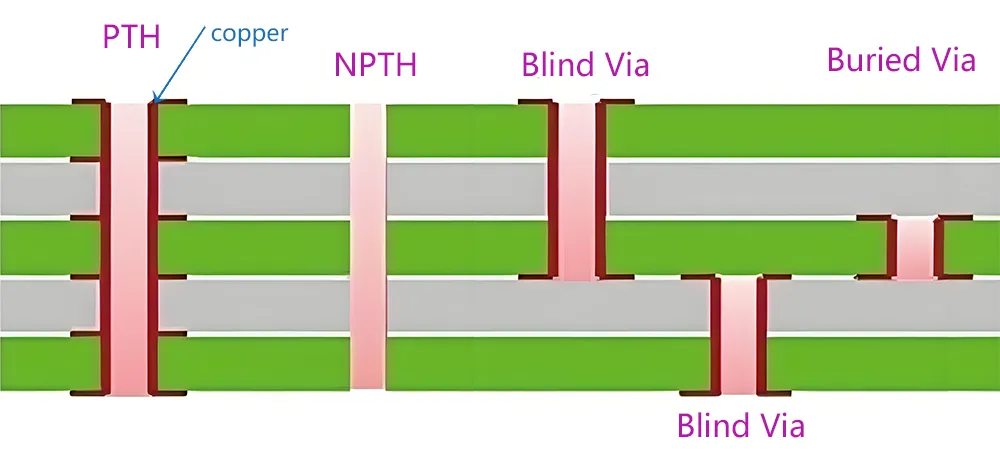
Type of PCB Drilling
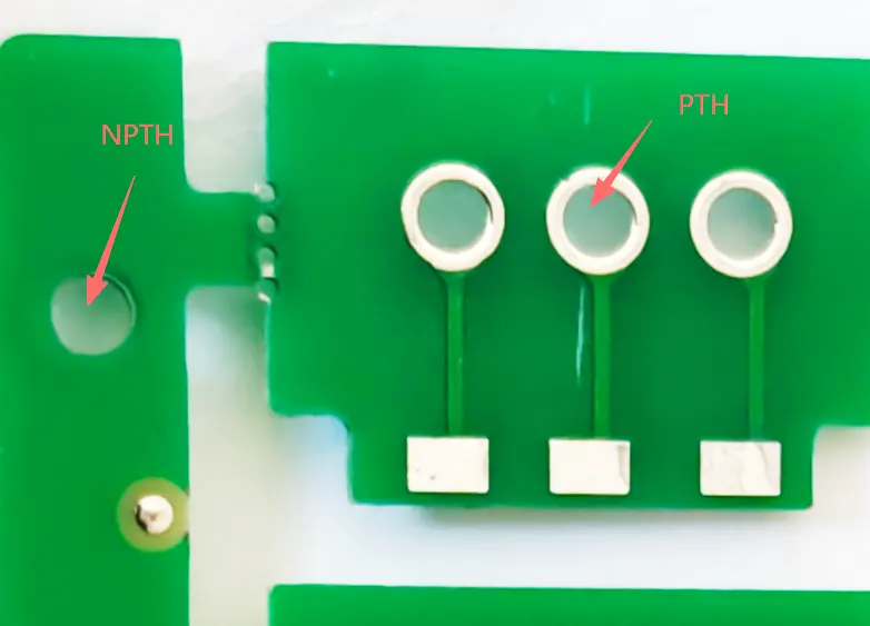
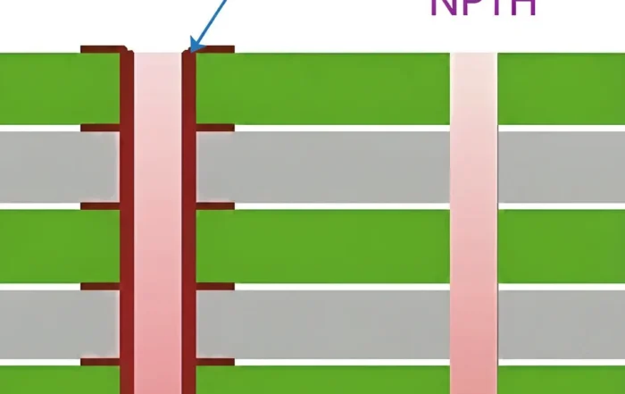
PTH and NPTH
Plated Through Holes (PTH)
PTHs are the most common holes in PCBs, where the inner wall of the hole is coated with conductive copper plating.
- They provide electrical connectivity between the top, bottom, and inner copper layers.
- The hole wall integrity and copper plating thickness directly affect the reliability of the board.
For flexible circuit boards, engineers must carefully manage hole wall integrity to prevent cracking under bending or thermal cycling.
Hole type decides the drilling method, so designers should label each one. The common categories are:
| Hole type | Function | Typical drilling route |
|---|---|---|
| Through-hole (PTH) | Connects all copper layers | Mechanical, 0.15 mm and up |
| Blind via | Reaches an outer layer only | Mechanical or laser |
| Buried via | Stays inside the stack | Mechanical or laser |
| Microvia | Links adjacent layers in HDI | Laser, 0.1 mm and below |
| Via-in-pad | Places the via inside a pad | Laser, then fill and plate |
| Component hole | Holds connectors or heat sinks | Mechanical |
In a Rigid-Flex PCB, blind and buried vias often share the stack with through-holes. Layer count and bend areas then limit routing space, as explained in Rigid-Flex PCB Technology.
Non-Plated Through Holes (NPTH)
These holes are used for mechanical purposes such as mounting components or the s.
NPTH does not have any copper plating.
They do not participate in the electrical performance of the PCB.
Reference post: Plated and Non-Plated Through Hole
Key Drilling Parameters that Influence Quality
Drilling is a high-speed, precision process. Each parameter impacts the final board quality and cost:
Drill Bits: Shorter, more rigid bits reduce deflection and positional inaccuracy.
Spindle Speed: Higher RPMs improve cutting but may increase heat. It must be tuned based on the material.
Feed Rate: If too fast, it causes smearing or cracking; if too slow, it lowers productivity.
Depth Control: Essential for blind and buried vias—over-drilling ruins the layer below.
Desmear Process: Chemical removal of resin to ensure copper plating adheres well.
Hole Diameter Tolerance: Must be tightly maintained to fit component leads and plating requirements.
Step-by-Step: PCB Drilling Process Flow
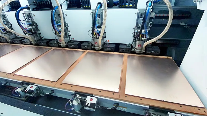
Here’s how PCB manufacturers execute precision drilling:
Panel Fixation: Secure the rigid or flex panel using fixtures.
Pre-Drilling: Use short blades to test alignment.
Main Drilling: Execute full-depth drilling using mechanical or laser tools.
Deburring: Remove smears and roughness from drilled holes.
Desmear: Clean resin residue chemically (e.g., KMnO₄).
Plated Through Hole (PTH) Process: Electroless copper followed by electroplating.
Quality Inspection: Inspect hole wall smoothness, positional accuracy, and CPK metrics.
Reference post: PCB Drilling Process: The Cornerstone of Precision
Key Drilling Parameters That Affect Hole Quality in PCB Manufacturing
In high-precision PCB manufacturing, particularly for multilayer and HDI designs, drilling quality has a direct impact on electrical performance and long-term reliability. Several critical parameters influence the final hole integrity, copper plating adhesion, and via functionality. Optimizing these drilling parameters is crucial to maintaining tight tolerances and ensuring robust interconnections.
Here’s a summary of the most impactful drilling parameters:
| Drilling Parameter | Effect on Hole Quality |
|---|---|
| Drill Bits | Using short, rigid drill bits minimizes deflection, improving hole position accuracy. |
| Spindle Speed | Higher RPM increases cutting efficiency but generates more heat, risking resin smear. |
| Feed Rate | Too fast can cause delamination, smearing, or cracks; too slow leads to low productivity. |
| Depth Control | Critical for blind and buried vias to avoid overdrilling and ensure layer-specific contact. |
| Desmear Process | Chemical resin removal (e.g., KMnO₄) ensures clean walls and optimal adhesion of copper plating. |
| Diameter Tolerance | Maintaining design tolerances is vital to ensure proper component fit and soldering. |
You must carefully adjust each of these parameters during the PCB drilling process. This ensures the final product meets IPC standards for via reliability and electrical performance. Poor control of drilling conditions can lead to open circuits, low plating quality, or misalignment. This is especially true in flexible or rigid-flex PCB applications with dense layer stacking.
Mechanical vs. Laser: Choosing the Right Drill for PCB Board
| Factor | Mechanical Drilling | Laser Drilling |
|---|---|---|
| Hole Size | ≥ 0.15 mm | ≤ 0.1 mm (microvias) |
| Cost | Lower equipment, higher wear | High initial investment |
| Speed | Moderate | Ultra-fast (ideal for HDI) |
| Accuracy | Moderate | Extremely high |
| Suitable Applications | PTH, standard boards | HDI, flex circuits, micro-components |
| Thermal Impact | High | Low (safe for flex materials) |
Takeaway: For high-density or flex PCBs, laser is not optional—it’s essential. For low-cost, low-density boards, mechanical is still viable.
Reference post: PCB Laser Drilling: A Comprehensive Guide
Flex PCB Drilling Quality: What Changes on Flexible Substrates
A Flexible PCB behaves differently under a drill. The substrate stretches, so mechanical drilling can distort the panel or tear the copper. Vacuum fixtures hold the panel flat and reduce that risk.
Laser drilling suits thin dielectrics well, which helps flex PCB drilling quality. There is no contact force, so the polyimide stays flat and microvias land on target. Still, debris removal and burr height need checking on every lot.
Because flex panels are thin, handling matters as much as the drill program. Support carriers, controlled stack heights, and gentle clamping all protect hole edges. Buyers in medical and automotive programs often pair these steps with High-Reliability Flexible Circuits for High-End Applications.
Inspection, Defects and Acceptance Criteria
Inspection closes the loop. AOI catches missing or misplaced holes on outer layers. X-ray reveals buried and blind vias inside the stack. Cross-sectioning shows hole wall roughness, smear, and copper plating thickness, while the annular ring is measured from the same cut.
Acceptance is usually written, not implied. Many programs agree on targets against IPC-6012 Class 2 or Class 3. That standard covers hole wall quality, annular ring, and copper registration. True position measurement confirms that holes sit where the design placed them.
Common defects and their fixes:
| Defect | Root cause | Fix |
|---|---|---|
| Nailheading | Aggressive feed, worn bit | Lower feed, change bit sooner |
| Smear | Heat and poor chip removal | Adjust retract, improve vacuum |
| Pad lift | Excess heat on thin laminate | Cut spindle speed, add backup |
| Drill breakage | High hit count, deep hole | Cap hits, use a pilot hole |
| Misregistration | Tooling or fiducial error | Re-check pins and alignment |
| Burr | Dull tool on soft substrate | Sharpen schedule, lower force |
Routine PCB testing methods such as coupon cross-sections catch drift before it reaches a full panel. Sampling plans should match the class and volume of the order. For document requests, the PCB Manufacturing FAQ covers common drilling and plating questions.
Conclusion: Optimizing Drilling for Today’s PCB Demands
As electronics evolve, so does the complexity of PCBs. High-speed signals, tighter spaces, and flexible formats demand precision drilling. Choosing between mechanical and laser drilling depends on hole size, board type, and performance needs.
At Gekun, we use both methods based on your needs. This ensures high quality, speed, and cost-efficiency for every printed circuit board.
FAQ
What is the difference between laser and mechanical drilling in PCBs?
Mechanical drilling cuts with a rotating carbide or diamond-coated bit and handles holes of 0.15 mm and up. Laser drilling removes material with a CO₂ or UV beam, adds no contact force, and makes microvias of 0.1 mm and below. Hole size, material, and volume decide the choice.
What is the smallest hole each method can produce?
Laser drilling reaches microvias of 0.1 mm and below. Mechanical drilling is used for holes of 0.15 mm and above. Designs that need smaller openings usually move to a laser source.
How do you check flex PCB drilling quality?
Check three things: hole position against the design, hole wall and burr condition under cross-section, and debris removal after drilling. Flex PCB drilling quality also depends on panel support, so inspect for stretching or copper damage near bend areas.
Why do drill bits wear or break?
Bits wear with hit count and abrasive glass content. Heat and poor chip evacuation speed up the damage. Broken bits usually trace back to high hit counts, deep holes, or worn tools.
Does the drilling method affect cost and yield?
Yes. Mechanical drilling has lower equipment cost but needs regular bit replacement. Laser drilling costs more upfront and runs faster on small holes. Matching the method to hole size and volume keeps yield high.
Related Posts
- PCB Testing Methods: 8 Techniques for Quality Assurance — Related article
- Improve PCB Micro-Drill Performance on Flex Boards — Related article
- Rigid-Flex PCB Drilling Burr Reduction Technology — Related article
- Flexible PCB: Features, Design Guide & Applications — Related article