
Flexible PCB for Smart Glasses: Design, Hinge Bend & Assembly Guide

A flexible PCB for smart glasses is a thin polyimide circuit that carries power, camera, audio, sensor, and display signals through the temples and frame. It bends at the hinge every time the wearer folds the glasses. This flexible PCB for smart glasses guide covers materials, bend rules, stackup budgets, DFM checks, and assembly in steps you can hand to a fabricator.
See also Industrial Automation for related specifications.
See also FPC for Mobile Phones for related specifications.
See also FPC for Consumer Electronics for related specifications.
See also High-Reliability Flexible Circuits for High-End Applications for related specifications.
What a Flexible PCB Does Inside Smart Glasses
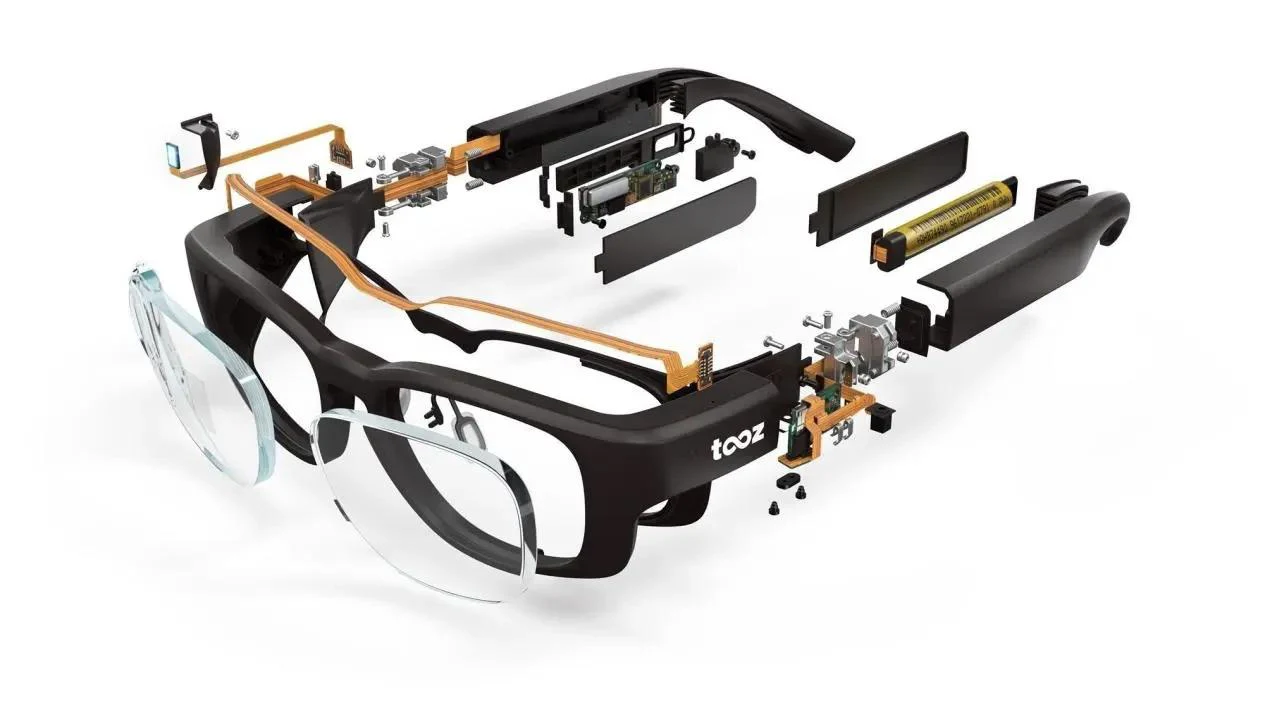
Smart glasses squeeze a camera, a waveguide display driver, touch temples, a microphone, a 2.4 GHz radio, and a 1S lithium-polymer battery into two narrow arms. No single rigid board fits that shape. Designers therefore split the electronics into small rigid islands and join them with flex tongues.
A typical build has three electronic blocks:
- Front frame: camera module, display driver, ambient light sensor.
- Temple (left or right): SoC, memory, radio and antenna.
- Rear temple: battery, charging contacts, speaker.
The flex circuit connects these blocks without board-to-board connectors. This saves space and removes one connector-related failure point. For broader background, read the flexible PCB technology guide first.
Why Flexible Circuits Fit Eyewear Better Than Rigid Boards
Eyewear is a mechanical product as much as an electronic one. Temples fold, frames flex, and users expect near-zero weight. Flex circuits answer all three demands.
- Thin profile. A two-layer flex with coverlay is often 0.2 mm thick, so it hides inside a 3–4 mm temple wall.
- Hinge compliance. The flex becomes the moving joint between frame and temple, replacing a fine-wire harness.
- Fewer connectors. Direct soldering to stiffened pads cuts cost and vibration risk.
- Design freedom. Traces route around the lens cut-out and the nose bridge curve.
In addition, flex absorbs shock better than a stiff board. The trade-off is that every bend must be designed and tested, not discovered on the bench. This Flexible PCB overview explains the underlying construction.
Material Selection: Match the Material to the Bend
Material choice drives bend life, reflow survivability, and cost. Use the table below as a first filter, then confirm the build with your fabricator.
| Option | Best use | Bend life | Relative cost |
|---|---|---|---|
| Polyimide (PI) + adhesive coverlay | Dynamic hinge bends | High | Medium |
| PI + photo-imageable coverlay | Fine pitch, tight bends | High | Medium-high |
| PET | Static bends, no reflow | Low | Low |
| Thin modified FR4 | Rigid islands only | None | Low |
| FR4 or stainless stiffener | Connector and camera pads | Not applicable | Low |
Three rules matter most. First, use polyimide with rolled-annealed (RA) copper in every dynamic zone, because RA copper resists fatigue far better than electro-deposited copper at the same thickness. Second, keep coverlay adhesive at 25 µm or thinner in the bend, since thick adhesive builds stress. Third, reserve PET and thin FR4 for static areas such as the battery pocket.
Material Decision Tree by Bend Radius, Reflow Count and Cost Tier
Use a short decision sequence instead of a generic material-is-important discussion:
1. Classify the zone. Mark every region as dynamic hinge, static fold, or rigid island. Dynamic zones drive the material choice.
2. Calculate the bend radius. Divide the available cavity depth by 2 to estimate the maximum radius, then compare with the 10:1 dynamic ratio. If the ratio falls below 10:1, reduce stack thickness before changing material.
3. Count reflow exposures. If the flex sees more than two reflow cycles, eliminate PET. Use PI with RA copper and a coverlay that matches the assembly temperature profile.
4. Apply the cost tier. Low tier: static PET or thin FR4, one copper layer, no fine pitch. Medium tier: two-layer PI, RA copper, adhesive coverlay, simple stiffener. High tier: four-layer rigid-flex, photo-imageable coverlay, gold finish and tight bend tolerance.
5. Confirm with the fabricator. Request a stackup drawing with real material part numbers and reflow compatibility data before releasing Gerbers.
Dynamic Bend Life at the Temple Hinge
The hinge is the main fatigue location. Every open-and-close action reverses the bend, so the flex sees cyclic strain rather than a one-time static fold. Design the hinge as a dynamic bend from the first layout review.
Start with the bend ratio. IPC-2223 guidance starts near a 10:1 bend radius to total thickness for dynamic flex, and about 5:1 to 6:1 for static bends. A 0.2 mm stack at 10:1 therefore needs a 2 mm radius. If the temple design cannot provide 2 mm, reduce copper thickness, reduce coverlay adhesive, or move the bend line away from the hinge barrel.
Estimate the cycle count from user behavior. A light pair folded 20 times a day for three years needs about 22,000 cycles. A heavier usage model of 50 folds a day for five years needs about 91,000 cycles. Specify at least two times the calculated life with margin, and push toward a 20:1 bend ratio when the target exceeds 100,000 cycles.
Validate the dynamic bend with a fold fixture, not a static bend test:
1. Build a representative stack. Use the same copper, adhesive, and coverlay as production, including the stiffener and rigid-flex transition.
2. Set the fixture to the real hinge angle. Cycle between the open and closed positions at 1–2 Hz.
3. Log trace resistance continuously. A 10% rise signals an incipient crack. Stop and inspect the bend line under magnification.
4. Run at least the calculated life plus margin. A common target is 50,000 cycles for a light pair and 100,000 cycles for a daily-heavy product.
5. Repeat after thermal cycling. Fatigue life drops when adhesive stiffness changes, so test the bend after the thermal profile.
Add a mechanical stop so the temple cannot fold past its design angle. Over-rotation is the fastest way to crack a flex, and no material choice can compensate for an uncontrolled hinge.
Design Rules for the Hinge Bend
Treat the hinge as a dynamic bend with a defined cycle target, not a one-time fold.
1. Set the bend ratio. IPC-2223 guidance starts near a 10:1 bend radius to total thickness for dynamic flex, and about 5:1 to 6:1 for static bends. A 0.2 mm stack at 10:1 therefore needs a 2 mm radius.
2. Route traces perpendicular to the bend line. Angled traces concentrate strain. Fan out, then run straight through the bend.
3. Stagger the traces. Keep at least one trace width of gap, and keep copper off the panel edge.
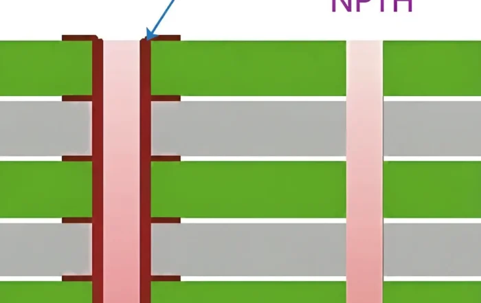
4. Never place vias in the bend zone. Plated holes act as stress risers.
5. Use arcs, not 90° corners. Radius every inner corner of the flex outline.
6. Add a service loop. A small slack curve absorbs tolerance stack-up at the hinge barrel.
7. Keep stiffener, solder mask, and large pads out of the bend.
Also add a mechanical stop so the temple cannot fold past its design angle. Over-rotation is the fastest way to crack a flex.
Stackup and Thickness Budget
Temple walls are usually 3–4 mm thick, and the internal cavity is often under 1.5 mm. Plan the stackup before layout.
| Stackup | Construction | Typical total thickness | Bend performance |
|---|---|---|---|
| 1-layer flex | 1/2 oz RA copper, 25 µm PI, 25 µm coverlay | ~0.12 mm | Highest |
| 2-layer flex | 1/2 oz copper, 25 µm PI core, adhesive, coverlay | ~0.20–0.25 mm | High |
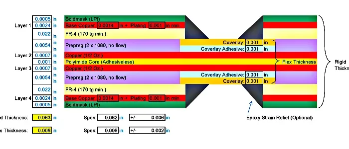
| 4-layer flex | Two cores with no-flow prepreg | ~0.35–0.45 mm | Medium |
| Rigid-flex | 2-layer flex plus FR4 islands | 0.6–0.8 mm at islands | Medium |
These values are typical, not guaranteed. Your fabricator should confirm them against the real copper and adhesive build. In addition, the rigid-to-flex transition needs 1.5–2 mm of gradual relief, or the coverlay will lift. A step above 0.3 mm between rigid and flex creates a stress point.
Space Budget by Location
Use a mechanical budget table before routing. Confirm every value against the real CAD envelope and fabricator capability.
| Location | Typical available depth | Recommended flex stack | Rigid-flex transition length |
|---|---|---|---|
| Hinge barrel | 0.6–1.0 mm | 0.12–0.25 mm | 1.5–2 mm relief each side |
| Temple cavity | 1.0–1.5 mm | 0.20–0.25 mm | 1.5–2 mm |
| Front frame | 0.8–1.5 mm | 0.12–0.35 mm | 1.5–2 mm |
| Battery pocket | 1.0–2.0 mm | 0.20–0.45 mm | 2 mm |
Example Two-Layer Hinge Stackup
A practical example is a two-layer flex with 1/2 oz RA copper, a 25 µm polyimide core, 25 µm adhesive, and a 25 µm coverlay. The finished thickness is about 0.20–0.25 mm. At a 10:1 bend ratio, this needs a 2.0–2.5 mm radius. If the hinge barrel cannot provide that radius, move to a one-layer flex at about 0.12 mm or reduce the copper and adhesive thickness.
Rigid-Flex Partitioning in Five Steps
1. Partition the rigid islands. Group the SoC, memory, and radio on one island. Put the battery and charging contacts on another. Keep high-speed routing inside an island.
2. Cross the hinge with a dedicated flex tongue. Give the tongue its own outline and keep it narrow. A 4–6 mm tongue is common for a camera plus power bundle.
3. Set the stackup and total thickness early. Changing layer count later breaks the impedance plan.
4. Design camera pads and surface finish. Use gold plating or ENIG on camera and connector pads. Add a stiffener behind the pad field to stop pad lift.
5. Control MIPI impedance. Camera and display links usually need 100 Ω differential. Keep a continuous ground reference and never split the reference under a pair.
Steps 4 and 5 cause most re-spins. Review them with the fabricator before releasing Gerbers.
Form-Factor Scenarios: Camera, Waveguide, Touch Temple and Battery Interconnect
Smart glasses are not a single generic wearable. Each module places different constraints on the flex.
Camera Module Interconnect
The camera sits in the front frame and usually feeds a MIPI link to the temple SoC. Use a short, narrow flex tongue with a stiffener behind the sensor pad field. Keep the bend line out of the pad area, and route the differential pair perpendicular to the hinge bend. Add a ground pour under the pair, and do not place the camera flex under the antenna keep-out.
Waveguide Display Driver
The waveguide driver often sits at the frame edge near the lens cut-out. The flex may follow a curved path around the nose bridge, but the dynamic bend should stay at the hinge. Keep the driver and its decoupling capacitors on a rigid island, use thermal vias under the driver, and avoid routing the display pair across a split in the ground reference.
Touch Temple
A touch temple uses capacitive electrode traces along the inside of the arm. Route the sensing traces with a symmetric pattern, add guard traces tied to the same reference, and keep them away from the battery and charging current paths. If the touch flex crosses the hinge, place the sensing electrodes outside the high-stress bend zone and use a service loop for tolerance.
Battery Interconnect
The battery interconnect carries the highest current in the product. Use wide copper, parallel runs, and a ground pour to hold IR drop under 2%. Put the charging IC on a rigid island with thermal vias. At the battery pocket, add strain relief and a service loop so wire movement does not peel the pads. Test the pack under charge and discharge while monitoring connector and flex temperature.
Low Power, Heat and Antenna Coexistence
Flex circuits in eyewear face three electrical constraints:
- Power delivery. Battery current flows through narrow traces. Use wide copper, parallel runs, and a ground pour to hold IR drop under 2%.
- Thermal spread. Polyimide conducts heat poorly. Therefore, add copper pour and thermal vias under the display driver and charging IC, and keep the battery below its 45 °C charge limit.
- Antenna clearance. Metal hinges and the flex ground plane detune 2.4 GHz antennas. Keep the antenna keep-out free of copper and stay 3–5 mm from hinge metal.
Flex Layout Constraints for Power, Heat and RF
Translate the constraints into layout rules:
- Power: calculate IR drop on the longest battery-to-SoC path before routing. Add copper width or a second layer before adding a connector.
- Heat: place thermal vias in a 2–3 mm grid under the charging IC and display driver. Do not rely on the polyimide alone to spread heat.
- RF: keep the antenna keep-out free of copper, stiffener, and coverlay openings. Do not route display or camera pairs under the antenna. Stitch the ground around the RF section, but avoid creating a ground loop through the hinge metal.
- Mechanical: keep the antenna zone away from the bend, because a flexing ground plane changes tuning.
Test all three on a prototype with the real temple material. Plastic and metal temples behave differently.
Failure Modes to Design Out Early
Most field returns in wearables trace back to a few causes. Watch for these before tooling:
| Failure mode | Root cause | Design countermeasure |
|---|---|---|
| Trace fracture at the bend line | Tight radius, angled traces, thick copper | Raise bend ratio, re-route perpendicular, use RA copper at 1/2 oz or lower |
| Coverlay delamination or blistering | Thick adhesive, sharp rigid-flex step, trapped moisture | Use thin adhesive, add 1.5–2 mm relief taper, bake before reflow |
| Pad peel under connectors | No stiffener, weak pad anchoring, thermal mismatch | Add stiffener behind pad field, anchor pads with teardrops, match adhesive CTE |
| Stiffener release | Adhesive mismatch after thermal cycling | Match adhesive CTE and cure profile, keep stiffener out of bend |
| Solder crack at camera or battery pad | Rigid pad field on a moving flex | Move the pad field to a rigid island, add strain relief and service loop |
This flexible PCB failure modes review lists more causes and fixes. Pair it with the Flexible PCB Design Mistakes checklist during design review.
DFM Checklist and Prototype Validation
Before release, confirm each item:
- Bend radius at least 10× stack thickness in every dynamic zone.
- No vias, pads, or stiffeners inside the bend zone.
- Copper at 1/2 oz or lower in the bend zone.
- Coverlay openings at least 0.5 mm clear of the bend outline.
- Continuous ground reference under every differential pair.
- Teardrops on every pad-to-trace junction.
- Rigid-flex transition relief of 1.5–2 mm on each side.
Then validate with real hardware:
1. Fold fatigue. Cycle 10,000–100,000 folds at 1–2 Hz while logging trace resistance. A 10% rise signals an incipient crack.
2. Thermal cycling. Run −40 °C to +85 °C for 100–500 cycles, then inspect the rigid-flex transition.
3. Damp heat. Hold at 85 °C and 85% RH for 500 hours to check adhesive stability.
4. Sweat and salt spray. Artificial perspiration and salt fog test the finish and exposed copper.
5. Drop and torsion. Eyewear gets sat on more often than it gets dropped.
Manufacturing and Assembly Notes
Fabrication follows standard steps: copper lamination, imaging, etching, coverlay lamination, surface finish and electrical test. The Flexible PCB Process Guide explains each stage and the tolerances to expect.
Assembly is where thin parts fail. The Flexible PCB SMT process guide covers panel handling, stiffener placement and reflow profiles. In addition, Flexible Circuit Board Assembly Equipment Design explains the fixtures and carriers that keep 0.2 mm parts flat.
Practical points:
- Panelize onto a carrier and keep bare flex away from printers.
- Use no-flow prepreg for rigid-flex and control lamination pressure.
- Bake parts before reflow to remove absorbed moisture.
Cost Factors and Supplier Selection
Cost drivers, ranked by impact:
1. Layer count and stiffener count.
2. Tight bend-radius tolerances and outline complexity.
3. Surface finish — gold plating costs more than ENIG.
4. Test coverage — full electrical test pays off on wearables.
5. Volume and panel utilization.
Cost Tiers by Design Choice
- Low tier: one-layer static flex, PET or thin FR4, no stiffener, simple outline.
- Medium tier: two-layer PI flex with RA copper, adhesive coverlay, one stiffener, and standard ENIG.
- High tier: four-layer rigid-flex, photo-imageable coverlay, gold finish, tight bend-radius tolerance, and full electrical test.
Supplier Selection Process
When you compare suppliers, ask for bend-cycle data, an IPC-2223-based DFM report, and a stackup drawing with real material part numbers. A supplier that answers with numbers is safer than one that answers with adjectives. Confirm these points in the quote stage:
1. Stackup capability: can the supplier build the copper, adhesive, and coverlay thickness you specified?
2. Dynamic bend experience: has the supplier tested a similar stack at your target radius and cycle count?
3. Rigid-flex transition control: what relief length and lamination pressure does the supplier use?
4. Reflow compatibility: can the material survive your assembly profile without coverlay blistering?
5. Panelization and test: does the quote include carrier design, electrical test, and traceability?
What Comes Next
The direction is clear: thinner stacks, finer lines, and better end-of-life handling. Closed-loop recycling is moving from concept to pilot, and a Closed-Loop Recyclable Flexible PCB build now targets material recovery instead of landfill. Expect 4-layer flex and embedded components to become standard as display drivers demand more routing.
FAQ
What is a flexible PCB for smart glasses?
It is a thin polyimide circuit that carries power and signals through the frame and temples of smart glasses. It flexes at the hinge when the glasses fold, replacing wires and board-to-board connectors. Typical builds are 0.12–0.45 mm thick and use one to four copper layers.
How small a bend radius can a smart glasses flex use?
Use at least 10× the total stack thickness for a dynamic hinge bend and 5–6× for a static bend. A 0.2 mm stack therefore needs about a 2 mm radius at the hinge. Higher fold-cycle targets, above 100,000 cycles, usually push the ratio to 20:1 or more.
How many fold cycles should a hinge flex survive?
Match the cycle target to product life. A light pair folded 20 times a day for three years needs about 22,000 cycles, so specify at least 50,000 with margin. Validate with a 1–2 Hz fold test that logs resistance, and treat a 10% rise as an early crack signal.
Which material is best for the hinge bend?
Polyimide with rolled-annealed copper and a thin adhesive coverlay is the standard choice. RA copper resists fatigue better than electro-deposited copper. Keep adhesive at 25 µm or less in the bend. PET and thin FR4 are cheaper but suit static zones only, and PET cannot survive reflow.
How thick should a temple flex be?
Most temple cavities accept a 0.2–0.25 mm two-layer flex. One-layer flex at about 0.12 mm gives the longest bend life, while 4-layer flex at 0.35–0.45 mm is used when routing density demands it. Rigid-flex islands run 0.6–0.8 mm and need 1.5–2 mm of transition relief.
Glossary
- Bend ratio: bend radius divided by total flex thickness.
- Coverlay: the polyimide plus adhesive layer that protects flex traces.
- Stiffener: an FR4 or metal patch that keeps pads flat.
- Rigid-flex: a board with rigid islands joined by flex sections.
- Service loop: deliberate slack that absorbs hinge movement.
Related Posts
- Flexible PCB Technology Guide: Materials & Design — Related article
- Flexible PCB: Features, Design Guide & Applications — Related article
- Closed-Loop Recyclable Flexible PCB Manufacturing Guide — Related article
- Flexible Circuit Board Assembly Equipment Design Guide — Related article
- Flexible PCB Design Mistakes to Avoid | Gekun FPC Guide — Related article