
Copper Foil Types and Thickness Selection of Flex PCB
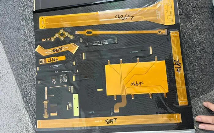

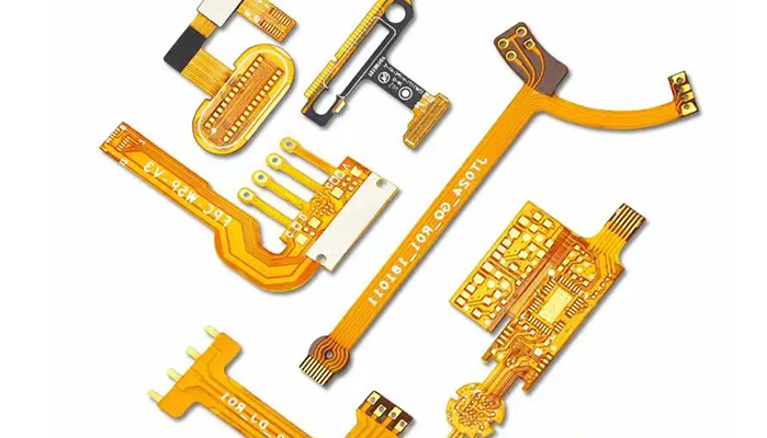
When engineers discuss flexible printed circuit board (Flex PCB) design, attention often focuses on substrate materials, bend radius, trace routing, or layer count. However, one of the most influential factors affecting long-term performance is frequently overlooked: the copper foil itself.
Introduction: Why Copper Foil Determines the Success of a Flex PCB
Copper foil serves as the conductive backbone of every flexible circuit. It carries electrical signals, delivers power, dissipates heat, and endures mechanical deformation during bending and flexing.
While the polyimide substrate provides flexibility, the copper layer ultimately determines whether a flex circuit can survive thousands—or even millions—of bending cycles without failure.
Many premature flex PCB failures can be traced back to improper copper selection. Excessively thick copper may improve current-carrying capacity but significantly increases bending stress.
Likewise, selecting the wrong copper foil type can lead to fatigue cracking, conductor fracture, or delamination during repeated flexing.
These issues become particularly critical in applications such as foldable electronics, medical devices, automotive systems, and wearable technology, where reliability is non-negotiable.
The relationship between copper type, copper thickness, flexibility, and service life is highly interconnected.
A thinner copper foil generally improves flexibility and fatigue resistance, whereas thicker copper enhances conductivity and thermal performance.
Similarly, different manufacturing methods produce copper foils with distinct grain structures that directly affect bending endurance.
This guide explores the engineering principles behind copper foil selection for flexible PCBs.
It explains the major copper foil types, compares their performance characteristics, and discusses how thickness influences electrical and mechanical behavior.
By understanding these factors, designers can make informed decisions that balance flexibility, reliability, and cost.
Understanding the Role of Copper Foil in Flex PCB Construction
Where Copper Foil Sits in a Flex PCB Stack-Up
A flexible PCB consists of multiple functional layers working together to provide electrical performance and mechanical flexibility. Among these layers, copper foil serves as the conductive element that forms the circuit traces.
A typical single-sided flexible PCB stack-up includes the following layers:
| Layer | Function |
|---|---|
| Coverlay | Protects circuitry from moisture, abrasion, and contamination |
| Copper Foil | Forms conductive traces and pads |
| Polyimide Substrate | Provides flexibility and mechanical support |
| Adhesive (optional) | Bonds copper and coverlay to the substrate |
In modern adhesive-free constructions, copper foil is directly bonded to the polyimide film, reducing overall thickness and improving flexibility.
This approach is widely used in high-performance flex and rigid-flex applications where bending reliability is critical.
The position of the copper layer within the stack-up significantly affects mechanical behavior during flexing.
Because copper has a much higher modulus of elasticity than polyimide, it experiences most of the tensile and compressive stress generated during bending.
As a result, copper foil selection becomes a key factor in determining the mechanical durability of the circuit.
What Copper Foil Actually Does
Although copper foil is primarily viewed as an electrical conductor, its role extends far beyond simply carrying current.
The most obvious function is electrical conduction. Copper possesses one of the highest electrical conductivities among commercially available metals, approximately 5.96 × 10⁷ S/m at room temperature.
This allows electrical signals and power to travel through the circuit with minimal resistance losses.
Copper foil also determines the current-carrying capability of a flexible circuit. Increasing copper thickness increases the cross-sectional area of conductors, reducing resistance and enabling higher current flow.
This characteristic becomes particularly important in power electronics, battery management systems, and automotive applications.
Signal transmission is another critical function. High-speed digital systems and RF circuits require stable transmission paths with controlled impedance and minimal signal loss. The surface characteristics and thickness of copper foil directly influence conductor resistance, skin effect behavior, and overall signal integrity.
In flexible circuits, copper additionally serves a mechanical function. During bending, the copper layer must withstand repeated tensile and compressive stresses without cracking.
Unlike rigid PCBs, where copper remains largely stationary, flex PCB copper experiences continuous mechanical deformation throughout its operational life.
Table 1 summarizes the primary functions of copper foil in flexible circuit design.
| Function | Impact on PCB Performance |
|---|---|
| Electrical Conductivity | Enables efficient current flow |
| Signal Transmission | Maintains signal integrity |
| Thermal Management | Helps dissipate heat |
| Mechanical Durability | Resists fatigue during bending |
| Structural Support | Maintains trace geometry |
Why Copper Foil Selection Is More Critical in Flex PCBs Than Rigid PCBs
Copper selection is important in all printed circuit boards, but its significance increases dramatically in flexible circuits.
In rigid PCBs, copper traces remain fixed and experience little mechanical stress during normal operation. As long as electrical and thermal requirements are satisfied, copper selection has relatively limited influence on long-term reliability.
Flex PCBs operate under entirely different conditions. Many applications require continuous movement throughout the product lifecycle.
Examples include folding smartphones, laptop hinges, automotive camera modules, medical endoscopes, and wearable electronics.
Every bending cycle introduces tensile stress on one side of the copper conductor and compressive stress on the opposite side.
Over time, these repeated stress cycles can initiate microscopic cracks that gradually propagate through the conductor. Eventually, the copper trace fractures, resulting in circuit failure.
Dynamic bending applications are particularly demanding.
Industry testing has shown that copper grain structure, foil thickness, and bend radius all play significant roles in determining fatigue life. In many cases, a small reduction in copper thickness can dramatically improve bending endurance.
Another challenge involves space constraints. Modern electronic products continue to shrink in size while increasing functionality. Designers often require ultra-thin circuits capable of fitting into compact assemblies without sacrificing reliability.
This trend places even greater emphasis on selecting the optimal copper foil type and thickness.
Consequently, copper foil selection in flex PCB design is not merely an electrical decision. It is a multidisciplinary engineering decision involving electrical performance, mechanical reliability, thermal management, manufacturability, and product lifespan.
Two Main Copper Foil Types Used in Flex PCBs
Flexible PCBs primarily utilize two categories of copper foil: Rolled Annealed (RA) copper and Electrodeposited (ED) copper. Although both materials consist of high-purity copper, their manufacturing methods create significantly different microstructures and mechanical properties.
Understanding these differences is essential when designing circuits that must endure bending and flexing.
Rolled Annealed (RA) Copper
Rolled Annealed copper is produced by mechanically rolling copper ingots into thin sheets followed by an annealing process. During annealing, the material is heated and slowly cooled to relieve internal stresses and improve ductility.
This manufacturing process creates elongated grain structures aligned along the rolling direction. The resulting microstructure provides exceptional flexibility and fatigue resistance.
Compared with other copper foil types, RA copper exhibits superior elongation properties, often exceeding 20% elongation before fracture.
This characteristic allows the material to tolerate repeated bending without developing cracks.
As a result, RA copper has become the preferred choice for dynamic flex applications where circuits must withstand continuous movement.
Typical applications include:
- Foldable smartphones and tablets
- Wearable electronics
- Medical imaging probes
- Automotive steering-wheel controls
- Camera modules with moving assemblies
- Rigid-flex PCB hinge sections
Although RA copper delivers outstanding mechanical performance, its manufacturing process is more complex and costly than electrodeposition methods, resulting in a higher material price.
Electrodeposited (ED) Copper
Electrodeposited copper is manufactured through an electroplating process. Copper ions are deposited onto a rotating cathode drum, gradually forming a thin copper foil layer.
Unlike RA copper, ED copper develops a columnar grain structure that grows perpendicular to the foil surface. This structure provides excellent dimensional consistency and supports fine-line circuit fabrication.
One major advantage of ED copper is its cost efficiency. The electrodeposition process enables large-scale production with relatively low manufacturing costs, making it widely used throughout the PCB industry.
ED copper also offers smoother surface characteristics, which can be advantageous for fine-pitch etching and high-density interconnect designs.
However, its lower ductility limits its performance in dynamic flex applications. Repeated bending may eventually cause grain boundary cracking, reducing fatigue life compared with RA copper.
Consequently, ED copper is typically used in applications where the circuit remains relatively stationary after installation.
Common examples include:
- LED lighting modules
- Static flex circuits
- Consumer electronics
- Display interconnections
- Cost-sensitive products
RA vs. ED Copper: Which One Should You Choose?
The selection between RA and ED copper depends primarily on the mechanical demands of the application.
For circuits subjected to frequent flexing, RA copper consistently provides superior reliability due to its excellent elongation and fatigue resistance. For static or low-cycle applications, ED copper often delivers sufficient performance at a lower cost.
Table 2 compares the key characteristics of both copper foil types.
| Property | RA Copper | ED Copper |
|---|---|---|
| Manufacturing Method | Rolling + Annealing | Electrodeposition |
| Grain Structure | Horizontal / Elongated | Vertical / Columnar |
| Flexibility | Excellent | Moderate |
| Fatigue Resistance | Excellent | Lower |
| Fine-Line Etching | Good | Excellent |
| Cost | Higher | Lower |
| Dynamic Flex Applications | Highly Recommended | Not Recommended |
| Static Flex Applications | Suitable | Suitable |
For most dynamic-flex designs, industry best practice favors RA copper despite its higher cost.
The additional material expense is often insignificant compared with the long-term reliability benefits and reduced risk of field failures.
Flex PCB Copper Thickness Explained
Copper foil thickness is one of the most influential design parameters in flexible circuit engineering. It affects electrical conductivity, current-carrying capacity, heat dissipation, flexibility, bend radius, and fatigue life.
Selecting the appropriate thickness requires balancing electrical performance with mechanical durability.
Copper Thickness Units
The PCB industry commonly expresses copper thickness using three measurement systems: ounces per square foot (oz/ft²), micrometers (μm), and mils.
The ounce system originates from the weight of copper distributed across one square foot of area.
Although somewhat unconventional, it remains the most widely used standard in PCB manufacturing.
The following conversion table illustrates common relationships.
| Copper Weight | Thickness (μm) | Thickness (mil) |
|---|---|---|
| 1/3 oz | 12 μm | 0.47 mil |
| 1/2 oz | 18 μm | 0.71 mil |
| 1 oz | 35 μm | 1.37 mil |
| 2 oz | 70 μm | 2.76 mil |
These values represent nominal thicknesses before additional plating processes are applied.
Common Flex PCB Copper Thicknesses
Flexible circuits typically use thinner copper foils than rigid PCBs to maximize flexibility and reduce bending stress.
| Thickness | Copper Weight | Typical Applications |
|---|---|---|
| 12 μm | 1/3 oz | Ultra-flexible wearable devices |
| 18 μm | 1/2 oz | Consumer electronics and mobile devices |
| 35 μm | 1 oz | General-purpose flex circuits |
| 70 μm | 2 oz | Power distribution and high-current applications |
Among these options, 18 μm and 35 μm copper are the most commonly specified in commercial flex PCB manufacturing because they provide a practical balance between flexibility and electrical performance.
How Thickness Influences Flexibility
Copper thickness has a direct and measurable impact on the mechanical behavior of a flexible circuit.
As thickness increases, the conductor becomes stiffer and less capable of accommodating bending deformation.
During flexing, thicker copper experiences higher strain levels, accelerating fatigue damage and increasing the likelihood of crack formation.
Conversely, thinner copper allows strain to distribute more evenly across the conductor, significantly improving bending endurance and service life.
This creates an engineering trade-off. Thick copper improves conductivity, current capacity, and thermal performance, while thin copper enhances flexibility and fatigue resistance.
For dynamic-flex applications, designers generally prioritize flexibility and choose thinner copper foils.
For power-intensive applications where current carrying capability is the dominant requirement, thicker copper becomes necessary despite the reduction in bending performance.
The most successful flex PCB designs achieve an optimal balance between electrical and mechanical requirements rather than maximizing either property alone.
Relationship Between Copper Thickness and Bend Radius
In flexible circuit design, copper thickness cannot be evaluated independently. Its effect on reliability becomes apparent only when considered together with bend radius. Even a high-quality copper foil can fail prematurely if the bending radius is too small for its thickness.
The relationship between copper thickness and bend radius is one of the most important considerations in flex PCB engineering because it directly determines the strain experienced by the conductor during operation.
Why Copper Cracks During Repeated Flexing
Many engineers assume copper fails because it is repeatedly bent. In reality, failure occurs because repeated bending generates cyclic mechanical stress within the conductor.
When a flexible circuit bends, the outer surface of the copper stretches while the inner surface compresses. These opposing forces create mechanical strain throughout the conductor.
Tensile Stress
The outer side of the bend experiences tensile stress. Copper atoms are pulled apart as the conductor elongates. If the strain exceeds the material’s elastic limit, microscopic cracks begin forming along grain boundaries.
Over thousands or millions of bending cycles, these cracks gradually grow until the conductor fractures completely.
Compression Stress
The inner side of the bend experiences compression stress. Instead of stretching, the copper is squeezed together.
Although compression is generally less damaging than tension, excessive compressive stress can contribute to conductor buckling, delamination, or deformation of adjacent dielectric layers.
Copper Fatigue
The primary failure mechanism in dynamic flex circuits is metal fatigue.
Metal fatigue occurs when repeated loading causes microscopic structural damage that accumulates over time. Unlike overload failures, fatigue can occur even when individual stress cycles remain well below the ultimate strength of the material.
For example, a wearable medical sensor may flex only a few degrees during each movement. However, after several million cycles, fatigue cracks can still develop if the copper foil is not properly selected.
Research and IPC flex circuit guidelines consistently show that fatigue life improves significantly when designers use thinner copper foils and larger bend radii.
The following table illustrates the general relationship between copper thickness and flex endurance.
| Copper Thickness | Relative Flexibility | Relative Fatigue Life |
|---|---|---|
| 12 μm | Excellent | Very High |
| 18 μm | Excellent | High |
| 35 μm | Good | Moderate |
| 70 μm | Limited | Low |
Although actual fatigue life depends on many variables, thinner copper generally survives substantially more bending cycles than thicker alternatives.
Neutral Axis Theory Simplified
Understanding neutral axis theory helps explain why copper thickness has such a profound impact on flex PCB reliability.
When a flexible circuit bends, not all layers experience the same amount of strain. Somewhere within the structure exists an imaginary plane known as the neutral axis.
At the neutral axis, material neither stretches nor compresses.
Layers located above the neutral axis experience tensile stress, while layers below it experience compressive stress.
What Designers Need to Know
The farther a copper layer sits from the neutral axis, the greater the strain it experiences during bending.
In single-layer flex circuits, the copper conductor is often located relatively close to the outer surface of the structure. This positioning increases the amount of mechanical stress applied to the conductor during flexing.
Modern flex PCB stack-ups often use symmetrical constructions and adhesive-free laminates to move the copper closer to the neutral axis and reduce stress concentration.
This design approach can dramatically improve fatigue resistance without changing conductor geometry.
How Thickness Changes Stress Distribution
Copper thickness directly influences strain levels because thicker conductors occupy a larger distance from the neutral axis.
The strain generated during bending can be approximated by:
Strain (%) = t / (2R) × 100
Where:
- t = total circuit thickness
- R = bend radius
This equation demonstrates a simple but important principle:
When copper thickness increases, strain increases proportionally.
When bend radius increases, strain decreases proportionally.
For example, reducing copper thickness from 35 μm to 18 μm can significantly reduce conductor strain under identical bending conditions.
This is why thin copper foils dominate high-flex applications such as foldable electronics and wearable devices.
Recommended Copper Thickness for Different Bend Conditions
Copper thickness recommendations should always be based on the expected mechanical environment.
Different applications impose dramatically different flexing requirements.
Static Bend Applications
Static bends occur when a circuit is bent once during installation and then remains in a fixed position.
Examples include:
- Printer interconnects
- Automotive dashboards
- Industrial control panels
Since the circuit rarely moves after assembly, fatigue resistance is less critical.
Copper thicknesses between 18 μm and 35 μm are commonly used in these applications.
Dynamic Bend Applications
Dynamic flex circuits bend repeatedly throughout their service life.
Examples include:
- Laptop hinges
- Camera modules
- Foldable consumer devices
These applications require significantly better fatigue performance.
Most manufacturers recommend using RA copper with thicknesses of 12 μm to 18 μm whenever possible.
Continuous Motion Applications
Some applications operate under constant movement and may experience millions of flex cycles.
Examples include:
- Medical endoscopes
- Robotic cable systems
- Wearable health monitors
For these demanding environments, ultra-thin RA copper is typically the preferred solution.
Table 4 summarizes typical recommendations.
| Application Type | Typical Flex Cycles | Recommended Copper Type | Typical Thickness |
|---|---|---|---|
| Static Bend | <100 | ED or RA | 18–35 μm |
| Dynamic Bend | 10,000–1,000,000 | RA | 12–18 μm |
| Continuous Motion | >1,000,000 | RA | 12 μm or thinner |
The key principle remains consistent: as flexing frequency increases, copper thickness generally decreases.
Choosing Copper Foil Based on Real-World Applications
Selecting copper foil based solely on thickness or cost often leads to suboptimal results. The most successful designs begin with application requirements and then determine the appropriate copper foil characteristics.
Different industries prioritize different performance objectives, including flexibility, durability, miniaturization, thermal performance, and cost efficiency.
Wearable Electronics
Wearable devices represent one of the most demanding categories of flex PCB applications.
Smart watches, fitness trackers, smart clothing, and health-monitoring patches must withstand constant movement while maintaining compact dimensions.
In these products, flexibility and fatigue resistance are generally more important than high current capacity.
Because wearable devices frequently bend with body movement, RA copper is typically preferred.
Copper thicknesses of 12 μm or 18 μm are commonly selected to maximize flexibility and minimize fatigue stress.
| Requirement | Preferred Solution |
|---|---|
| Continuous movement | RA copper |
| Thin profile | 12 μm copper |
| Long fatigue life | RA copper |
| Lightweight design | 12–18 μm copper |
Foldable Consumer Devices
Foldable smartphones, tablets, and laptops have transformed flex circuit design requirements.
Unlike traditional electronics, these products repeatedly fold and unfold throughout their lifespan. Some premium devices are designed to survive more than 200,000 folding cycles.
To meet these reliability targets, manufacturers commonly specify ultra-thin RA copper combined with adhesive-free laminate structures.
Typical copper thicknesses range from 12 μm to 18 μm.
The combination reduces strain concentration and allows tighter bend radii without conductor failure.
Medical Devices
Medical electronics place a strong emphasis on reliability because failures may directly affect patient safety.
Applications such as endoscopes, catheter systems, portable diagnostic equipment, and patient monitoring devices frequently employ flexible circuits.
Endoscopes and catheter systems require exceptional bending endurance because they operate in highly constrained environments.
Portable diagnostic devices may prioritize miniaturization and signal integrity.
Patient monitoring systems often require a balance between flexibility and durability.
For these applications, RA copper is typically selected because of its superior fatigue resistance and predictable mechanical performance.
Automotive Flex Circuits
The automotive industry presents a unique combination of mechanical, thermal, and environmental challenges.
Flexible circuits appear in:
- Steering wheel controls
- Rear-view camera systems
- Battery management systems
- Advanced driver-assistance systems (ADAS)
Steering systems and camera modules often involve movement and vibration, making RA copper advantageous.
Battery connection circuits may require thicker copper due to higher current demands.
Consequently, automotive applications frequently use copper thicknesses ranging from 18 μm to 70 μm depending on electrical requirements.
Industrial and Robotics Applications
Industrial automation equipment increasingly relies on flexible circuits to reduce wiring complexity and improve reliability.
Applications include robotic arms, motion-control systems, machine vision equipment, and sensor assemblies.
These environments often combine continuous movement with harsh operating conditions.
Robotic cable assemblies may experience millions of bending cycles over their operational life.
As a result, engineers frequently specify RA copper combined with optimized bend radius designs.
For sensor circuits and signal transmission applications, 12 μm to 18 μm copper typically provides sufficient electrical performance while maximizing durability.
Common Copper Foil Selection Mistakes That Reduce Flex PCB Life
Many flex PCB failures can be prevented during the design phase. Unfortunately, several common mistakes continue to appear in production designs.
Using Thick Copper in Dynamic Bend Areas
One of the most frequent design errors is specifying thick copper throughout the entire circuit.
While thicker copper improves current capacity, it also increases stiffness and bending strain.
In dynamic-flex regions, excessive copper thickness often becomes the root cause of premature conductor fatigue.
Selecting ED Copper for High-Cycle Applications
ED copper may reduce material costs, but its columnar grain structure provides lower fatigue resistance than RA copper.
For products expected to endure thousands or millions of flex cycles, selecting ED copper can significantly reduce service life.
The initial cost savings are often outweighed by reliability issues later.
Ignoring Bend Radius Requirements
Even the best copper foil cannot compensate for an excessively tight bend radius.
Designers occasionally focus on conductor dimensions while neglecting mechanical constraints.
Following IPC flex design recommendations for minimum bend radius is essential for achieving long-term reliability.
Focusing Only on Current Capacity
Electrical requirements should never be considered in isolation.
A copper thickness chosen solely for current carrying capability may create unnecessary mechanical stress.
Successful flex PCB designs balance electrical performance, thermal requirements, flexibility, and fatigue life simultaneously.
Overlooking Manufacturing Constraints
Manufacturing limitations can influence copper selection just as much as performance requirements.
Factors such as etching capability, trace width tolerance, plating processes, laminate availability, and cost targets all affect the practicality of a design.
Early collaboration with PCB manufacturers often helps identify potential issues before production begins.
Table 5 summarizes common design mistakes and their consequences.
| Design Mistake | Potential Consequence |
|---|---|
| Excessively thick copper | Reduced flexibility and shorter fatigue life |
| ED copper in dynamic applications | Premature conductor cracking |
| Small bend radius | Increased strain and failure risk |
| Current-focused design only | Mechanical reliability issues |
| Ignoring fabrication limitations | Manufacturing yield problems |
By avoiding these common pitfalls, engineers can significantly improve flex PCB durability while maintaining the electrical performance required by modern electronic products.
A Step-by-Step Copper Selection Workflow for Engineers
Selecting copper foil for a flexible PCB is rarely a matter of choosing the thinnest or most flexible option. Every design involves trade-offs among electrical performance, mechanical durability, manufacturability, and cost. Engineers who follow a structured decision-making process can avoid many of the reliability issues commonly encountered in flex circuit development.
The workflow below provides a practical framework for selecting the most appropriate copper foil for a given application.
Step 1: Define Current Requirements
The first consideration should always be electrical performance.
Copper thickness directly influences conductor resistance and current-carrying capability. As conductor cross-sectional area increases, resistance decreases, allowing more current to flow while generating less heat.
For low-power signal circuits, ultra-thin copper foils may provide sufficient conductivity while maximizing flexibility. Conversely, battery connections, power distribution networks, and motor-control systems often require thicker copper to safely handle higher current levels.
Table 6 provides a general guideline for selecting copper thickness based on application type.
| Application Category | Typical Current Level | Common Copper Thickness |
|---|---|---|
| Signal Circuits | <1 A | 12–18 μm |
| Consumer Electronics | 1–3 A | 18–35 μm |
| Automotive Electronics | 3–10 A | 35–70 μm |
| Power Electronics | >10 A | 70 μm and above |
Electrical requirements establish the minimum acceptable copper thickness, which becomes the starting point for further evaluation.
Step 2: Determine Bending Frequency
Mechanical movement is often the most important factor in flex PCB design.
A circuit that bends only once during installation experiences vastly different stresses than one operating continuously in a robotic assembly or foldable smartphone.
Designers should estimate the expected number of bending cycles throughout the product’s lifetime.
The following classification is commonly used:
| Flex Category | Typical Cycle Count |
|---|---|
| Static Flex | Less than 100 |
| Dynamic Flex | 10,000–1,000,000 |
| Continuous Flex | Greater than 1,000,000 |
As bending frequency increases, fatigue resistance becomes increasingly important, making RA copper the preferred choice.
Step 3: Identify Environmental Conditions
Environmental factors can significantly affect long-term reliability.
Flexible circuits operating in medical devices, automotive systems, aerospace equipment, or industrial machinery often encounter temperature fluctuations, humidity, vibration, and chemical exposure.
For example, automotive electronics may experience temperatures ranging from -40°C to +125°C, while wearable devices must tolerate sweat, moisture, and continuous mechanical movement.
Environmental conditions influence not only copper foil selection but also laminate materials, coverlay construction, and surface finishes.
Table 7 highlights common environmental considerations.
| Environment | Key Design Concern |
|---|---|
| High Temperature | Thermal expansion |
| High Humidity | Corrosion resistance |
| Vibration | Fatigue durability |
| Chemical Exposure | Material compatibility |
| Outdoor Applications | Environmental aging |
Ignoring these factors during material selection often leads to premature field failures.
Step 4: Evaluate Available Space
Modern electronics continue to become thinner, lighter, and more compact.
As available space decreases, designers often face pressure to reduce circuit thickness without sacrificing performance.
Ultra-thin flex circuits used in smartphones, wearable electronics, and medical devices commonly utilize thinner copper foils to achieve aggressive packaging targets.
Reducing copper thickness may also improve flexibility by decreasing the total circuit thickness and lowering bending strain.
However, excessive thinning can increase conductor resistance and reduce current-carrying capability. Therefore, space limitations must be balanced against electrical requirements.
Step 5: Select Copper Type
Once electrical and mechanical requirements are understood, the appropriate copper foil type can be selected.
For static applications, both RA and ED copper can provide satisfactory performance.
For dynamic applications, RA copper is generally preferred because its elongated grain structure offers superior fatigue resistance.
Table 8 summarizes common selection criteria.
| Design Requirement | Recommended Copper Type |
|---|---|
| Lowest Cost | ED Copper |
| Fine-Line Circuitry | ED Copper |
| Dynamic Bending | RA Copper |
| High Reliability | RA Copper |
| Foldable Devices | RA Copper |
| Wearable Electronics | RA Copper |
Although ED copper remains widely used throughout the PCB industry, the reliability advantages of RA copper often justify its higher cost in demanding flex applications.
Step 6: Select Copper Thickness
After determining the copper type, engineers can optimize thickness according to both electrical and mechanical requirements.
A common mistake is selecting the thickest copper possible to maximize conductivity. While this approach reduces electrical resistance, it often creates unnecessary mechanical stress and reduces fatigue life.
The optimal thickness depends on application requirements.
| Copper Thickness | Typical Application |
|---|---|
| 12 μm | Wearables, foldable devices |
| 18 μm | Consumer electronics |
| 35 μm | General-purpose flex circuits |
| 70 μm | Power and automotive systems |
Successful designs seek the minimum copper thickness capable of meeting electrical requirements.
Step 7: Verify Reliability Targets
Before finalizing the design, engineers should verify that the selected copper foil can achieve the required service life.
This verification may include:
- Bend-cycle testing
- Thermal cycling tests
- Environmental stress screening
- Accelerated life testing
- Finite element analysis (FEA)
Reliability verification becomes particularly important for medical, automotive, aerospace, and industrial applications where field failures can have serious consequences.
By validating performance early in development, designers can reduce risk and avoid costly redesigns later.
Future Trends in Flex PCB Copper Foil Technology
As electronic devices continue to evolve, copper foil technology is advancing alongside them. Emerging applications such as foldable smartphones, wearable health monitors, autonomous vehicles, and high-speed communication systems are driving new material innovations.
Several trends are shaping the future of flex PCB copper foil development.
Ultra-Thin Copper Foils
One of the most significant trends is the adoption of ultra-thin copper foils.
Traditional flexible circuits commonly use 18 μm or 35 μm copper. Today, leading manufacturers are producing copper foils as thin as 9 μm and even 5 μm for advanced applications.
Ultra-thin copper reduces overall circuit thickness and improves flexibility, enabling tighter bend radii and longer fatigue life.
These materials are becoming increasingly important for wearable electronics and foldable consumer devices.
Low-Roughness Copper for High-Speed Signals
As signal frequencies increase, conductor surface roughness becomes a critical factor in signal integrity.
At high frequencies, electrical current tends to flow near the conductor surface due to the skin effect. Rough copper surfaces increase signal loss by creating longer current paths and greater resistance.
To address this issue, manufacturers are developing low-profile (LP), very-low-profile (VLP), and hyper-very-low-profile (HVLP) copper foils.
These materials support higher data rates while minimizing insertion loss, making them attractive for 5G, AI hardware, advanced computing systems, and high-speed interconnect applications.
Adhesive-Free Copper Laminates
Traditional flexible laminates often use adhesive layers to bond copper foil to polyimide substrates.
Although effective, adhesives can introduce reliability challenges such as thermal expansion mismatch, moisture absorption, and increased thickness.
Adhesive-free constructions eliminate these concerns by directly bonding copper to the substrate.
Benefits include:
- Improved dimensional stability
- Enhanced heat resistance
- Better fatigue performance
- Reduced overall thickness
As reliability requirements continue to increase, adhesive-free laminates are becoming the preferred choice for premium flex PCB applications.
Copper Foils for Foldable Electronics
Foldable smartphones, tablets, and laptops have created entirely new design requirements.
Flexible circuits in these products must survive hundreds of thousands of folding cycles while maintaining stable electrical performance.
To meet these demands, copper foil manufacturers are developing specialized RA copper materials with optimized grain structures and improved elongation characteristics.
These materials help minimize fatigue damage in ultra-small bending radii.
Advanced Materials for Next-Generation Wearables
Future wearable electronics will require flexible circuits that are thinner, lighter, and more durable than current solutions.
Researchers are actively exploring advanced conductor materials, including:
- Nanostructured copper
- Copper-alloy systems
- Stretchable conductive materials
- Hybrid metal-polymer conductors
Although conventional copper foil remains the dominant technology today, these emerging materials may further expand the capabilities of wearable and biomedical electronics in the coming years.
Conclusion
Best Copper Foil Is Not the Thickest One
Copper foil selection plays a central role in determining the electrical performance, flexibility, and long-term reliability of a flexible PCB.
Throughout this guide, one principle repeatedly emerges: the optimal copper foil is not necessarily the thickest, strongest, or most expensive option. Instead, it is the material that best aligns with the specific requirements of the application.
Engineers must match copper type to bending requirements. Dynamic applications generally benefit from the superior fatigue resistance of Rolled Annealed (RA) copper, while static applications may achieve acceptable performance using Electrodeposited (ED) copper.
Copper thickness should likewise be matched to electrical demands. Excessive thickness can reduce flexibility and shorten fatigue life, while insufficient thickness may compromise conductivity and thermal performance.
Successful flex PCB designs achieve a balance among reliability, flexibility, manufacturability, and cost. This balance is often established during the earliest stages of design, long before fabrication begins.
For this reason, copper foil selection should never be treated as a secondary consideration. Early material decisions influence virtually every aspect of circuit performance, from bend radius and service life to signal integrity and production yield.
As flexible electronics continue to expand into wearable technology, foldable devices, medical systems, automotive electronics, and industrial automation, the importance of informed copper foil selection will only continue to grow.
Final Takeaway
Choose copper foil based on how the flex PCB moves, not just how much current it carries.
A thorough understanding of copper type, thickness, bend radius, and fatigue behavior enables engineers to build flexible circuits that deliver reliable performance throughout the entire product lifecycle.
References
- IPC-2223D, Sectional Design Standard for Flexible Printed Boards.
- IPC-6013E, Qualification and Performance Specification for Flexible Printed Boards.
- IPC-FC-234, Flexible Circuit Technology Handbook.
- Joseph Fjelstad, Flexible Circuit Technology, 4th Edition.
- DuPont™ Pyralux® Flexible Circuit Design Guide.
- Rogers Corporation, Flex Circuit Design Recommendations.
- JX Advanced Metals, Copper Foil Technical Handbook.
- Tatsuta Electric Wire & Cable, Rolled Annealed Copper Foil Specifications.
- IEC 61189 Series, Test Methods for Electrical Materials and PCB Reliability Evaluation.
- ASTM E345, Standard Methods for Tension Testing of Metallic Foil Materials.