
Liquid Metal Flexible Circuits: High-Reliability 3D Printed PI-Based Encapsulation Technology
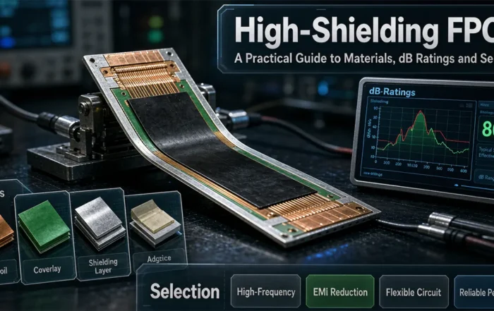
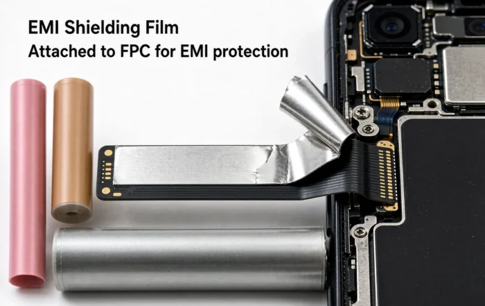
Liquid Metal Flexible Circuits combine a eutectic gallium-indium conductor with a polyimide (PI) substrate and cover layer. The PI layers fuse during 3D printing, so the wiring stays sealed when it bends, stretches, or heats up. This article explains the encapsulation process, the printing parameters that control it, the wetting and oxide controls that make it repeatable, and the checks that prove reliability at scale.
See also flexible PCB for LED face masks for related specifications.
Why Liquid Metal Flexible Circuits Need Better Encapsulation
The conductor is a eutectic gallium-indium alloy. It stays liquid at room temperature, melts below 30°C, and is non-toxic. It also maintains stable electrical and thermal conductivity, plus useful surface chemistry for soft devices.
Older soft conductors mix metal particles or ionic gels into elastomers. Their resistance shifts with humidity and temperature, so the circuit drifts. Liquid metal does not share that weakness. Therefore, it is a strong candidate for wearable devices and soft robotics.
The weak point sits in the package, not in the metal. A soft circuit fails when the cover layer loses contact with the substrate or when metal escapes. Encapsulation quality therefore decides the whole reliability story.
What the Literature Says About Liquid Metal Encapsulation
Reviews of gallium-based liquid metals and printed soft conductors consistently identify interface stability and oxide control as the dominant reliability variables. A 2018 Chemical Society Reviews review on liquid metals (500+ citations) and a 2017 Advanced Materials review on stretchable liquid metal electronics (1,000+ citations) both emphasize that the package, not the bulk alloy, sets fatigue life. A 2021 review of printable liquid metal composites (300+ citations) reaches the same conclusion for direct-write and screen-printed routes. These are not brand-specific claims; they are process signals that guide the PI encapsulation work below.
Limitations of Traditional Encapsulation Materials
Polydimethylsiloxane (PDMS) and Ecoflex are commonly selected as encapsulation materials for circuits. Although they exhibit good flexibility and tensile properties, the encapsulation layer and substrate layer cannot fuse well with these materials, making them prone to cracking.
Methods such as plasma treatment are required to enhance bonding; however, plasma processing causes certain damage to the materials, thereby reducing their mechanical strength.
During printing, PI enables mutual fusion between the substrate and encapsulation layers, achieving tight circuit encapsulation.
Compared to PDMS and Ecoflex, PI offers superior mechanical properties, dielectric performance, and excellent temperature resistance.
Proposed PI-Based Encapsulation Strategy
This study uses PI as both the flexible substrate and the encapsulation material. Printing one material on both sides produces integrated molding instead of a separate glued cover. During printing, PI enables mutual fusion between substrate and encapsulation layers, which delivers tight circuit encapsulation. For the wider material background, see PI-based flexible circuits.
There is a narrow process window. Too much PI solution lets organic solvents dissolve an incompletely imidized PI substrate. A little dissolution helps the layers fuse. Excessive dissolution weakens the substrate, and the circuit then sags or leaks. Both faults undermine packaging reliability and stability.
PI Coating and Curing Process Chain
The PI encapsulation chain should be specified as a recipe, not a single step:
1. Substrate preparation: start with a PI film or a printed PI precursor at 70–90% imidization. Clean with a mild solvent; avoid contaminating the bond surface.
2. Liquid metal printing: direct-write EGaIn at 1–20 mm/s with a 100–200 µm nozzle; immediately control the oxide with a brief acid vapor or formic acid wipe, then dry.
3. Encapsulation coating: apply PI solution by direct-write, slot-die, or screen coating to a wet thickness of 15–60 µm; target 10–40 µm after cure.
4. Stepped cure: ramp 2–5°C/min through 80°C/30 min, 120°C/30 min, 180°C/30 min, 250°C/60 min, and 300°C/30 min under nitrogen. For stacks that must preserve a partial-fusion window, stop at 250°C and finish after singulation.
5. Inspection: measure line width, cover thickness, insulation resistance, and peel adhesion before release.
The temperature curve matters because solvent must leave slowly enough to avoid bubbles but fast enough to avoid a weak, under-imidized cover. A final imidization above 95% gives the best dielectric and thermal stability; the substrate starts lower so the cover can partially dissolve and fuse into it.
Layer Thickness, Interfacial Adhesion, and Bend Durability
Cover thickness is a trade-off. A 10–20 µm cover is more compliant and preserves bend feel, but it leaves less margin against pinholes and leakage. A 25–40 µm cover gives a stronger leak barrier and better dielectric withstand, at the cost of stiffness. For most PI-based liquid metal flexible circuits, the reliable window is a 25–75 µm substrate with a 20–40 µm fused cover.
Interfacial adhesion should be judged by failure mode, not only by force. A good PI-PI fusion fails cohesively in the PI rather than peeling cleanly at the interface. Target a 90° peel test that shows cohesive failure, then confirm with 100,000 bending cycles at 2–3 mm radius and a resistance shift below 10%. If the failure is adhesive, the cover was under-cured, contaminated, or applied over a substrate that was too fully imidized to fuse.
How a 3D Printed PI Flexible Circuit Is Formed
The 3D printed PI flexible circuit is built as one stack, layer by layer:
1. Print the liquid metal wiring directly on the PI substrate.
2. Apply the PI encapsulation solution over the wiring.
3. Control encapsulation line width and substrate imidization degree.
4. Cure the stack so the substrate and cover layer fuse.
Each step is short, but steps two and three decide whether the circuit survives.
Line Width and Imidization Degree
Two parameters carry most of the risk. Encapsulation layer line width sets how much PI solution meets the substrate. Substrate imidization degree sets how much solvent the substrate can absorb before it softens.
This study regulates both together. The aim is optimal fusion without over-dissolving the substrate. Done correctly, the process prevents the sagging and leakage that follow excessive dissolution.
Wetting, Adhesion, and EGaIn Oxide Control on PI
EGaIn forms a thin gallium oxide skin (roughly 1–3 nm) immediately in air. That skin stabilizes the printed line, but it also raises the contact angle and can create insulating inclusions if it folds into the trace. On PI, the surface energy is moderate, so wetting is usually adequate after cleaning, but it is not self-optimizing.
Control strategy:
- Reduce oxide before deposition with brief HCl or formic acid vapor, then remove residues with nitrogen drying.
- Print in a low-oxygen glove box or with a local inert shroud when fine lines are required.
- Use a short, mild O2 plasma or corona on the PI only when the metal wetting angle remains too high; keep the treatment brief because aggressive plasma damages PI and hurts the later PI-PI fusion.
- Design a capture pad or dam at the trace edge to stop liquid metal spreading.
- Cure under nitrogen to limit oxide growth during the thermal cycle.
Adhesion of the metal to PI is mechanical plus oxide-mediated. The fused PI cover provides the real seal; the metal-PI interface only needs to survive handling and bending until cure.
Printing Parameters: Resolution, Conductivity, and Stretchability
The 3D printing window links geometry to electrical and mechanical output:
- Nozzle inner diameter: 100–200 µm is a practical range for EGaIn. Trace width is typically 0.8–1.5× the nozzle diameter; lines below 50 µm require a finer nozzle, lower flow, and tighter oxide control.
- Print speed: 1–20 mm/s. Higher speed narrows the trace and reduces bulge, but too high a speed causes necking and opens.
- Flow rate and pressure: 0.1–1.0 µL/min or 10–50 kPa. Higher flow fills voids and raises conductivity toward the bulk value, but overfill increases line width and leakage risk.
- Layer height: 0.05–0.2 mm for the PI cover. Thinner layers improve resolution but need more passes and more cure cycles.
- Conductivity: bulk EGaIn is about 3.4×10^6 S/m. Printed lines typically reach 70–90% of bulk when voids and oxide inclusions are controlled; the loss comes from porosity and oxide folding, not from the alloy itself.
- Stretchability: straight traces localize strain. Serpentine or horseshoe geometry plus a 20–40 µm fused cover gives the best bend and stretch margin. A thinner cover improves compliance but reduces leak margin.
The key trade is resolution versus conductivity. Fine lines need low flow and high speed, which increase the chance of opens. Thick, high-flow lines conduct better but are wider and harder to encapsulate without voids.
Scalable Manufacturing Routes: Screen Printing, Green Solvents, Sintering, and 3D Printing
Screen printing, green solvents, sintering, and 3D printing each solve a different scale problem.
| Route | Strength | Limit | Fit |
|---|---|---|---|
| Screen printing | High throughput, roll-to-roll, thick layers | Resolution usually 50–100 µm; stencil cost | Volume production of larger features |
| 3D printing | Digital, conformal, fine features, no mask | Slower; nozzle clogging; oxide control | Prototypes, high-mix, fine lines |
| Green solvents | Lower toxicity and recovery burden | May change PI imidization and fusion window | Pilot lines with solvent recovery |
| Sintering | Raises conductivity of particle inks | Extra thermal budget; not needed for EGaIn | Silver or copper particle inks, not liquid metal |
For liquid metal, sintering is not the conductivity lever; oxide control and void-free encapsulation are. Green solvents are useful only if they preserve the partial-fusion window. Screen printing can cut print time, but it cannot match direct-write resolution for fine PI encapsulation lines. A hybrid line often works best: screen print the coarse conductor or bond pads, then direct-write the fine encapsulation and traces.
Encapsulation Material Comparison
| Property | PDMS / Ecoflex | Polyimide (PI) |
|---|---|---|
| Fusion with substrate | Poor; needs extra bonding work | Fuses with the substrate during printing |
| Bonding treatment | Plasma, which can damage the material | Not required |
| Mechanical properties | Flexible and stretchable | Superior to PDMS and Ecoflex |
| Dielectric performance | Lower | Superior |
| Temperature resistance | Lower | Excellent |
The table shows the trade-offs the study accepts. PDMS and Ecoflex win on softness alone. PI wins on sealing, dielectric behaviour, and heat resistance, which matter more once the circuit must stay leak-free.
Reliability Checks for Liquid Metal FPC Encapsulation
Liquid metal FPC encapsulation should be judged at the interface first. A reliability plan should cover thermal cycling, damp heat aging, repeated bending, and insulation resistance or leakage current. Each test asks the same question: does the cover layer stay fused to the substrate?
Visual and electrical inspection should run alongside those tests. Look for circuit sag, metal leakage, and any separation between substrate and encapsulation layer. Failures usually trace back to over-dissolution during printing, not to the liquid metal itself.
Failure Modes and Yield
Failure modes cluster into four groups:
- Open trace: nozzle clog, oxide agglomerate, insufficient flow, or a neck at the print turn.
- Leakage: over-dissolution of the substrate, pinholes in a thin cover, or incomplete cure at the trace edge.
- Voids and bubbles: solvent outgassing, trapped air under the cover, or a cure ramp that is too fast.
- Delamination: under-cure, surface contamination, or a substrate that is too fully imidized to fuse.
Yield should be tracked with four tests: automated optical inspection for line width and cover voids, four-point resistance for opens, insulation resistance or leakage current for seals, and peel or bend test on coupons. A mature line should use statistical process control on nozzle pressure, print speed, cure temperature, and cover thickness. Most yield loss comes from the interaction of over-dissolution and voids, not from a single bad parameter.
Experimental Section
Primary Materials
Thermosetting PI, SG1020; Liquid Metal, DG-19.
Major Equipment and Instruments
Confocal Laser Microscope (CLM), VK-X1050, Keyence Corporation;
Vacuum Drying Oven, DZF-6050, Shanghai Yiheng Scientific Instrument Co., Ltd.;
Scanning Electron Microscope (SEM), JEOL JSM-5900LV, JEOL Trading Co., Ltd.;
Optical Microscope, S750, Meishi Di Dongguan Technology Co., Ltd.;
Electron Microscope, DM401, Shenzhen Yong’an Technology Co., Ltd.
Bending-Torsion Testing Machine, QL-5E, Xiamen Mid Electronics Technology Co., Ltd.;
Resistance Tester, RK2518-32, Shenzhen Meric Electronics Technology Co., Ltd.
Sample Preparation
The flexible circuit sample preparation process is shown in Figure 1.

Fig. 1 Flexible circuit sample preparation process
The specific workflow is as follows:
Step 1: Pre-treat the glass substrate.
Clean the glass substrate with anhydrous ethanol, then dry it in an 80°C vacuum oven for 5 minutes. Flatten and adhere the glass substrate to the printing substrate.
Step 2: Print the PI base layer.
Set appropriate flow rate and cycle parameters to ensure formation of an ideal liquid film morphology.
Step 3: Cure the PI base.
Perform isothermal heating curing under strictly controlled temperature and time conditions to achieve the desired imidization level and surface morphology.
Step 4: Print the circuit.
After adjusting printing parameters, activate the electrohydrodynamic inkjet 3D printing equipment to print liquid metal material, completing the fabrication of the flexible circuit.
Step 5: Print the PI encapsulation layer.
Set appropriate flow rate, speed, and voltage to print the PI imide encapsulation layer onto the circuit.
Step 6: Encapsulation Layer Curing.
Perform isothermal heating curing under strictly controlled temperature and time conditions to ensure uniform shrinkage of the encapsulation layer while maintaining the circuit morphology.
Fundamental Technical Principles
During flexible circuit manufacturing, the PI base layer is printed using direct material writing technology. As shown in Figure 2, the liquid overcomes viscous forces and surface tension under back pressure and gravity, extruding from the needle tip to form droplets that are precisely deposited onto the substrate.

Fig. 2 Material direct writing printing principle
Electrohydrodynamic Jet Printing of Circuits and Encapsulation Layers
As illustrated in Figure 3, circuits and encapsulation layers are printed using electrohydrodynamic jetting.

Fig. 3 Printing principle of electrohydrodynamic injection
The needle is held vertically downward to stabilize the jet stream, with the positive electrode connected to the needle tip and the negative electrode connected to the substrate, creating a strong electric field.
The electric field causes the liquid at the needle tip to accumulate charge, gradually forming a Taylor cone.
When the electric field strength is sufficiently high, the electric force overcomes the liquid’s surface tension and viscous forces, generating a fine jet.
During movement, the jet splits into minute droplets that ultimately deposit onto the substrate, forming the desired circuit or encapsulation layer.
Circuit Settlement and Leakage in Surface Encapsulation
Figure 4 reveals the settlement leakage process of the circuit under surface encapsulation and the cross-sectional morphology of the circuit after thermal curing. Initially, the liquid metal circuit is precisely printed onto the PI substrate [Figure 4(a)].

Fig. 4 Sedimentation leakage process of the circuit under surface package and the cross-sectional morphology of the circuit after heat curing
Subsequently, surface encapsulation and heating are performed [Figure 4(b)].
The PI substrate rapidly softens and then completely dissolves due to immersion in excess solvent molecules, causing the circuit to sink sharply [Figure 4(c)].
Ultimately, the liquid metal begins to leak out of the substrate layer [Figure 4(d)], threatening the integrity and stability of the flexible circuit.
The dissolution process ceases after thermal curing, halting circuit settling and leakage [Fig. 4(e)].
Figure 4(f) shows an SEM image revealing the cross-sectional morphology of the circuit under surface encapsulation.
Controlled Circuit Settlement with Wire Encapsulation
Figure 5 illustrates the settling process of the circuit under wire encapsulation and its cross-sectional morphology after thermal curing.

Fig. 5 The sedimentation process of the circuit in wire package and the cross-sectional morphology of the circuit after heat curing
The initial liquid metal circuit is printed onto a PI substrate [Figure 5(a)]. Line encapsulation is then performed, followed by heating [Figure 5(b)].
Subsequently, the PI substrate is immersed in an appropriate amount of solvent molecules to soften and dissolve [Figure 5(c)].
The line encapsulation ensures quantitative encapsulation of the PI solution, facilitating controlled circuit settlement and fusion between the substrate and encapsulation layer.
Upon complete solvent depletion, substrate softening and dissolution cease, halting circuit deposition.
The circuit remains largely fixed in position, though the PI substrate remains uncured [Figure 5(d)].
Final thermal curing fixes the liquid metal position, forming a stable circuit structure [Figure 5(e)].
Figure 5(f) shows the cross-sectional morphology of the circuit under wire encapsulation.
Key Mechanism of Wire-Encapsulation Technology
The key to wire-packaging technology lies in regulating the line width of the liquid PI encapsulation layer to control substrate dissolution and thereby modulate circuit deposition.
This lays the foundation for further controlling circuit deposition by adjusting the imidization degree of the PI substrate in subsequent steps.
From Lab to Production: Scale-up and Cost
Scale-up follows three stages:
1. Lab: single-nozzle direct write, manual cure, coupon testing. Cost is dominated by labor and inspection.
2. Pilot: multi-nozzle or array printing, automated cure profile, in-line AOI, solvent recovery. Cost shifts to yield and cycle time.
3. Production: roll-to-roll or panel processing, screen-printed coarse layers plus direct-write fine layers, closed-loop solvent handling.
A simple cost model is cost per good unit = (PI solution + liquid metal + print time + cure energy + inspection) / first-pass yield. At pilot volume, PI solution and printing time are often the largest material and cycle drivers; inspection can approach the printing cost if yield is low. Scale does not automatically reduce cost: if the cure profile is long or the nozzle clog rate is high, the line runs below capacity. The scalable levers are higher nozzle count, shorter stepped cure with verified imidization, solvent recovery, and design rules that keep trace width and cover thickness inside the proven window.
Results and Discussion
Control of Circuit Sinking
A comparison before and after circuit sinking is shown in Figure 6. The degree of imidization of the PI substrate layer and the amount of encapsulation layer applied critically influence liquid metal circuit settlement.
Therefore, the effects of substrate curing process parameters (heating temperature and time) and encapsulation layer line width on circuit settlement were investigated (Figure 7).
To control variables, the circuit line width was uniformly set at 150 (±5) μm.

Fig. 6 Comparison before and after circuit settlement

Fig. 7 Influence of process parameters on circuit settlement rate
Settlement Rate Calculation Method
Defined the formula for calculating the settlement rate:

Formula 1
In the formula:
H——Settlement rate, %
h1——Initial height, μm, as shown in Figure 6(a)
h2——Final height after settlement, μm, as shown in Figure 6(b)
Effect of Heating Temperature and Time
Figures 7(a) and (b) illustrate the effects of heating temperature and duration on circuit settlement in the PI substrate layer.
The encapsulation layer has a line width of 2 mm. At a heating time of 6 hours, increasing the temperature from 40°C to 80°C reduced the settlement rate from 85% to 8%. At 60°C, extending the heating time from 4 hours to 8 hours decreased the circuit settlement rate from 23% to 10%.
This indicates that as heating time and temperature increase, the substrate undergoes more thorough thermo-imidization, resulting in a more stable structure and enhanced support for the circuit. The circuit settlement rate decreased from 86% to 23%.
This indicates that as heating time and temperature increase, the substrate undergoes more thorough thermo-imidization, resulting in a more stable structure that provides enhanced support to the circuit and reduces the settlement rate.
Effect of Encapsulation Layer Line Width
Figure 7(c) reveals the relationship between the line width of the encapsulation layer and circuit settlement.
At 60°C and 6 hours, increasing the line width from 1.0 mm to 3.00 mm resulted in a rise in circuit settlement rate from 12% to 49%.
Increased line width implies higher PI solution consumption during encapsulation, intensifying the solution’s dissolution effect on the substrate layer.
This leads to a loosening of the substrate structure, weakening its circuit support function and consequently increasing the settlement rate.
Figure 7(d) shows the surface morphology of circuit settlement under SEM imaging.
The lowest controlled circuit settlement rate of 8% demonstrates that rational process coordination can significantly enhance the performance and quality of circuit encapsulation.
Effect of Process Parameters on PI Substrate Layer
The thickness and surface roughness of the PI substrate layer directly impact circuit printing quality as well as device comfort and thinness.
To ensure stable formation of the PI substrate layer and high-quality printing, it is necessary to investigate the effects of printing flow rate and cycle time on substrate layer thickness and surface roughness (Figure 8).

Fig. 8 Influence of process parameters on the thickness of PI base layer
Effect of Printing Parameters on PI Substrate Thickness
By exploring printing parameters, high-quality PI substrate layer printing can be achieved. Figure 8(a) shows that the thickness increases with rising print flow rate (300–700 μL/min).
An appropriate flow rate ensures continuous, stable substrate printing and surface smoothness.
Figure 8(b) illustrates the effect of stroke length (1–5 mm) on thickness. Results indicate that increasing stroke length consistently reduces thickness.
When exceeding 5 mm, print continuity is compromised, solution leveling becomes difficult, and a smooth film surface cannot be formed.
Formation Mechanism of the PI Base Layer
The surface roughness of the PI substrate layer is a critical indicator of print quality, significantly influenced by the print cycle and flow rate.
During printing, as shown in Figure 9, the liquid PI merges along the grid path to form a surface.

Fig. 9 Film formation principle of liquid PI base layer
Effect of Printing Cycle on Surface Roughness
As shown in Figure 10, the study investigated the effect of printing cycle (1–5 mm) on the surface roughness of the PI substrate layer, with a printing flow rate set at 500 μL/min.
Figure 10[(a)–(e)] depicts the CLM scanning topography of the substrate layer at different printing cycles.
As illustrated in Figure 10(f), surface roughness progressively increases with longer printing cycles. Increasing the printing cycle widens the line-to-line spacing.
If the solution’s flowability is insufficient to bridge the enlarged spacing, it impedes the leveling of the liquid film, leading to increased surface roughness.

Fig. 10 Influence of printing cycle on surface roughness of PI base layer
Effect of Printing Flow Rate on Surface Roughness
As shown in Figure 11, the effects of a printing cycle of 3 mm and printing flow rates (300–700 μL/min) on the surface roughness of the PI substrate layer were investigated. Figures 11(a) to (e) display the CLM scanning topography of the substrate layer at different printing cycles.
As shown in Figure 11(f), surface roughness progressively increases with higher printing flow rates.
The most pronounced increase occurred at 700 μL/min, where the color contrast in the CLM scanning morphology (Figure 11(e)) was most vivid, clearly indicating a significant rise in substrate surface roughness.
Excessive printing flow rates abnormally increase liquid film thickness, leading to uneven shrinkage during heating and curing, which in turn exacerbates roughness.

Fig. 11 Influence of print flow on surface roughness of PI base
Impact of Process Parameters on Circuit and Package Layer Line Width
Process parameters critically influence the line width of circuits and package layers. Therefore, the system systematically investigated the effects of printing voltage, flow rate, and speed (see Figures 12 and 13).

Fig. 12 Influence of process parameters on circuit width

Fig. 13 Influence of process parameters on line width of package layer
Printing voltage is critical for forming the Taylor cone jet and significantly affects the line width of circuits and encapsulation layers. As shown in Figure 12(a) and Figure 13(a), controlling the speed and flow rate parameters, the line width increases with higher voltage.
An appropriate voltage increase enhances the traction force exerted by the electric field on the liquid material, thereby ejecting more material onto the substrate.
As shown in Figure 12(b) and Figure 13(b), controlling voltage and flow rate parameters.
Line width decreases with increasing speed. Excessive speed leads to insufficient material supply, preventing continuous printing.
As shown in Figure 12(c) and Figure 13(c), controlling voltage and speed parameters. Line width increases with flow rate.
Higher flow rates result in a relative increase in extruded liquid material per unit time, leading to greater coverage area of material deposited on the substrate and consequently wider line widths.
Figure 12(d) specifically shows the line width morphology of the circuit under optical microscopy, while Figure 13(d) displays the morphology of the encapsulation layer under electron microscopy.
Electrical Stability of Flexible Circuits
The electrical stability of flexible circuits on PI substrates under bending conditions was investigated. Samples were clamped onto a testing machine for bending experiments.
As shown in Figure 14, L represents the original length of the flexible circuit sample, and d denotes the bending diameter of the circuit. Resistance changes were measured using an ohmmeter.

Fig. 14 Bending cycle test principle
The printed sample had a test length of 4 cm. The team conducted bending tests within a bending diameter range of 3.5–2 cm, repeating each test cycle 100 times. Figure 15 shows the results.

Fig. 15 Resistance change rate of flexible circuit under different bending states
Under bending deformation, the overall resistance change of the circuit remained minimal, and the resistance returned to its original value after each release of bending deformation.
In Figure 15(a), with a bending diameter of 3.5 cm, the resistance change rate ranged from 0.05% to 0.09%. Subsequently, in Figure 15(b), with a bending diameter of 3 cm, the resistance change rate ranged from 0.13% to 0. 18%.
Subsequently, at a bending diameter of 2.5 cm (Figure 15(c)), the resistance change rate ranged from 0.29% to 0.38%.
Finally, at a bending diameter of 2 cm (Figure 15(d)), the resistance change rate ranged from 0.40% to 0.54%.
The results of the bending cycle test indicate that the resistance change rate of the flexible circuit under cyclic bending strain does not exceed 0.54%, and the resistance change remains relatively constant within the same bending diameter.
This demonstrates that the manufactured flexible circuit maintains high stability even after repeated bending at different degrees.
Electrical Stability Under Torsion Conditions
The study clamped PI-based flexible circuit samples in a testing machine to investigate their electrical stability under torsion, as shown in Figure 16.

Fig. 16 Principle of the torsional loop test
Circuit samples underwent 100 cyclic torsions at various angles within the 90°–360° range, as illustrated in Figure 17.

Fig. 17 Resistance change rate of flexible circuit under different torsion states
Resistance changes remained negligible throughout torsion, with values consistently reverting to baseline after each cycle, further demonstrating exceptional electrical stability and reliability.
Resistance variations exhibited high consistency across hundreds of cycles at various angles, showing virtually no fluctuation from the original resistance value.
Torsion Test Results and Electrical Performance
Specifically: At 90° torsion [Figure 17(a)], the resistance change rate remained low at 0.12%–0.14%; At 180° torsion [Figure 17(b)], the resistance change rate slightly increased to 0.15%–0.19%.
At 270° torsion [Figure 17(c)], the resistance change rate increased to 0.29%–0.30%; at 360° torsion [Figure 17(d)], the resistance change rate reached its maximum but remained only 0.44%–0.45%.
The torsion cycle test demonstrates that the resistance change rate of the flexible circuit remains below 0.45% under cyclic torsion strain, with highly stable resistance variation at the same angle.
After enduring multiple torsion cycles of varying degrees, the flexible circuit maintains excellent stability and durability.
Applications and Manufacturing Outlook
Liquid metal circuits fit health monitoring, biomedical sensing, rehabilitation diagnostics, and soft robotics. These are exactly the fields where stiff copper flex is uncomfortable, and elastomer conductors drift. The same sealing logic supports high-reliability flexible circuits for high-end applications, wearable flex circuits, and LED face-mask flex circuits.
Using the aforementioned manufacturing method and process, the team designed and fabricated a PI-based flexible LED circuit board, as shown in Figure 18.
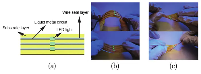
Fig. 18 PI‐based flexible LED circuit board
Figure 18(a) presents a schematic diagram of the PI-based flexible LED circuit board structure.
After thermal curing, the process completes the electronic device fabrication.
First, as shown in Figure 18(b), during bending tests in various directions, all three LEDs maintained stable illumination with highly consistent brightness.
Subsequently, as depicted in Figure 18(c), when subjected to torsion tests in different orientations, the three LEDs remained fully illuminated with brightness consistently preserved.
This demonstrates the device’s outstanding flexibility under complex deformation conditions, stable circuit connections, and exceptional mechanical durability.
Conclusion
(1) By regulating the line width of the encapsulation layer and the degree of imidization of the substrate, the process controlled substrate dissolution. This effectively managed the settlement of liquid metal circuits, achieving the lowest settlement rate of 8%.
This controlled settling stabilized the circuit’s position within the PI substrate, providing robust assurance for proper encapsulation and stable circuit operation.
(2) First, the study investigated the effects of print flow rate and cycle on PI substrate layer thickness and surface roughness.
Subsequently, the study explored the impacts of print voltage, speed, and flow rate on liquid metal circuit width and PI encapsulation layer line width.
By analyzing the trends in printing parameter effects, this provided crucial assurance for high-quality printing of the PI substrate layer, circuit layer, and encapsulation layer.
(3) After 100 cycles of bending at different diameters, the resistance change rate of the circuit samples did not exceed 0.54%; after 100 cycles of torsion at different angles, the resistance change rate did not exceed 0.45%.
In practical bending and torsion tests of PI-based flexible LED circuit boards in various orientations, all three LEDs maintained stable luminous states with highly consistent brightness.
Both electrical stability testing and practical applications demonstrate that the manufactured electronic devices exhibit excellent stability, high flexibility, and superior adaptability, confirming the feasibility and superiority of this technology.
FAQ
Are liquid metal flexible circuits stretchable?
The conductor is liquid at room temperature, so it deforms with the substrate instead of cracking. Overall stretch depends on the substrate and cover design. PI gives a stronger, better-sealed stack than PDMS or Ecoflex, while PDMS and Ecoflex stay softer.
Why use PI instead of PDMS or Ecoflex for liquid metal FPC encapsulation?
PI fuses with the substrate during printing, so no plasma treatment is needed. It also offers better mechanical properties, dielectric performance, and temperature resistance. PDMS and Ecoflex bond weakly and can crack at the interface.
What causes sag and leakage in a 3D printed PI flexible circuit?
Excess PI solution lets organic solvents dissolve an incompletely imidized substrate. Some dissolution is useful for fusion. Too much weakens the substrate, so the circuit sags and metal leaks. Controlling line width and imidization degree prevents both faults.
How is PI encapsulation cured for liquid metal flexible circuits?
Use a stepped cure with slow ramps: 80°C, 120°C, 180°C, 250°C, and 300°C under nitrogen, with holds long enough to remove solvent and complete imidization. The exact peak depends on whether the substrate needs a partial-fusion window. Fast ramps trap bubbles; under-cure causes delamination.
What printing parameters control resolution, conductivity, and stretchability?
Nozzle diameter and flow set line width and resolution. Higher flow and lower speed reduce voids and raise conductivity toward bulk EGaIn, but they widen the trace and raise leakage risk. Stretchability is set mainly by trace geometry and cover thickness: serpentine traces with a 20–40 µm fused PI cover perform best.
How do you control EGaIn oxide and wetting on PI?
Use brief acid vapor or formic acid to reduce the oxide skin, dry with nitrogen, and print in a low-oxygen environment for fine lines. Keep any plasma treatment on PI short, because aggressive plasma damages the surface and weakens the later PI-PI fusion.
What failure modes reduce yield?
The main modes are open traces from nozzle clog or oxide agglomerates, leakage from over-dissolution or pinholes, voids from solvent outgassing or fast cure, and delamination from under-cure or contamination. Track them with AOI, resistance, insulation, and peel tests.
Is PI-based liquid metal encapsulation scalable and cost-effective?
It can be, if the line moves from single-nozzle lab printing to multi-nozzle or hybrid screen-print plus direct-write production. Cost per good unit is driven by PI solution, print time, cure energy, inspection, and first-pass yield. Solvent recovery and design rules that stay inside the proven process window are the main cost levers.
Related Posts
- PI-based Flexible Circuit Optimization for Liquid Metal Printing — Related article
- Flex PCB Applications: Key Use Cases & Industries — Related article
- PI-Based Flexible Circuits Optimization — Related article
- What is FPC in Mobile? A Complete Guide to Flexible Circuits — Related article
- Flexible PCB: Features, Design Guide & Applications — Related article