Common Flexible PCB Failure Modes: Causes, Prevention, and Design Best Practices
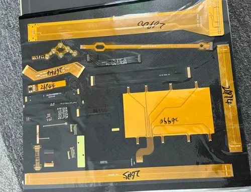
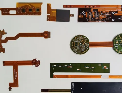
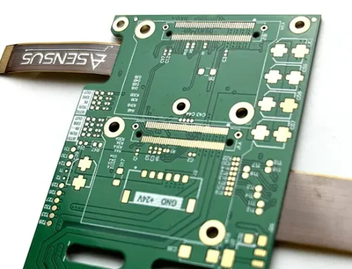
Flexible printed circuit boards (FPCBs) have become indispensable in modern electronics because they reduce weight, save space, and enable three-dimensional packaging. Industries such as consumer electronics, automotive, aerospace, industrial automation, and medical devices increasingly rely on flexible circuits to improve reliability while accommodating complex mechanical designs.
Despite these advantages, flexible PCBs experience failure mechanisms that differ significantly from those of conventional rigid boards. Unlike rigid PCBs, flexible circuits undergo continuous bending, twisting, vibration, and thermal cycling throughout their service life. If designers overlook these mechanical factors during product development, even a well-manufactured circuit may fail prematurely.
According to the IPC-2223 Design Standard for Flexible Printed Boards, most flex circuit failures originate from mechanical stress concentration rather than electrical defects. Studies published by NASA and the IPC also show that appropriate material selection, bend-radius control, and proper component placement dramatically improve long-term reliability.
This article examines the most common flexible PCB failure modes, explains why they occur, and outlines proven engineering practices that minimize failure risk.
Why Flexible PCBs Fail
Unlike rigid circuit boards that remain stationary, flexible circuits must repeatedly deform while maintaining electrical continuity. Every bending cycle introduces tensile and compressive stress into copper conductors, dielectric films, vias, and solder joints.
The primary factors that accelerate failure include:
| Failure Driver | Effect on Flexible PCB |
|---|---|
| Excessive bending | Copper fatigue and conductor cracking |
| Small bend radius | High localized mechanical strain |
| Thermal cycling | Expansion mismatch between materials |
| Vibration | Progressive fatigue around solder joints and vias |
| Moisture absorption | Delamination and blistering during reflow |
| Improper component placement | Stress concentration and pad lifting |
| Poor material selection | Reduced flex life and premature cracking |
Most failures develop gradually rather than suddenly. Small microscopic cracks expand through repeated mechanical loading until electrical continuity is lost.
Copper Trace Cracking and Fatigue
Copper trace fatigue is the most frequently reported failure mechanism in dynamic flex applications.
Each bending cycle slightly stretches the copper on one side of the neutral axis while compressing the opposite side. When the bend radius becomes too small, plastic deformation accumulates within the copper grains. Eventually, microscopic fatigue cracks develop and propagate through the conductor.
Primary Causes
The most common design mistakes include:
- Bend radius violations
- Routing traces perpendicular to the bend
- Using electrodeposited (ED) copper in dynamic applications
- Sharp corners in trace routing
- Excessive copper thickness
Rolled annealed (RA) copper possesses a grain structure aligned with the rolling direction, allowing it to tolerate significantly more bending cycles than electrodeposited copper. IPC therefore recommends RA copper for dynamic flex circuits.
Engineering Prevention
Designers can greatly increase flex life by following several proven practices.
| Best Practice | Benefit |
|---|---|
| Use RA copper | Higher fatigue resistance |
| Follow IPC-2223 bend radius guidelines | Reduces mechanical strain |
| Route traces parallel to bend direction | Lowers tensile stress |
| Replace sharp corners with curved routing | Eliminates stress concentration |
| Use thinner copper in dynamic regions | Improves flexibility |
For dynamic applications, IPC generally recommends minimum bend radii ranging from 10–20 times the circuit thickness, depending on layer count and construction.
Via Barrel Cracking
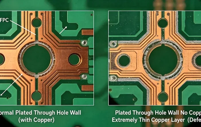
Vias provide electrical connections between conductive layers, but they also create localized regions of mechanical stiffness.
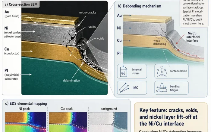
When vias are placed inside bending areas or immediately adjacent to rigid-flex transition zones, repeated deformation subjects the plated barrel to cyclic tensile stress. Eventually, microscopic fractures develop within the copper plating.
The problem becomes more severe because rigid FR-4 and flexible polyimide expand differently during temperature changes. Their differing coefficients of thermal expansion (CTE) continuously stress the plated hole walls.
Common Causes
| Design Issue | Result |
|---|---|
| Via inside bend area | Copper barrel fatigue |
| Via near rigid-flex transition | Stress concentration |
| Repeated vibration | Crack propagation |
| Large thermal cycling | Expansion mismatch damage |
Recommended Design Practices
Engineers generally avoid placing plated through holes inside flexible regions whenever possible.
Additional preventive measures include:
- Terminate blind and buried vias within rigid sections
- Increase the distance between vias and bend zones
- Reduce unnecessary layer transitions
- Maintain smooth rigid-flex transition geometry
These practices significantly improve long-term interconnect reliability.
Delamination and Blistering
Delamination occurs when copper foil, adhesive layers, coverlay, or dielectric films separate from one another.
The failure typically appears after solder reflow or prolonged thermal cycling.
The most common reason is moisture absorption. Polyimide materials naturally absorb moisture from the surrounding environment. During solder reflow, absorbed water rapidly expands into steam, generating internal pressure that separates bonded layers.
Other contributing factors include inadequate lamination pressure, poor adhesive quality, contamination, and excessive mechanical shear stress.
Typical Symptoms
- Raised blisters
- Layer separation
- Coverlay lifting
- Reduced insulation resistance
Prevention Methods
| Preventive Measure | Purpose |
|---|---|
| Bake boards before assembly | Removes absorbed moisture |
| Store in moisture barrier packaging | Reduces humidity exposure |
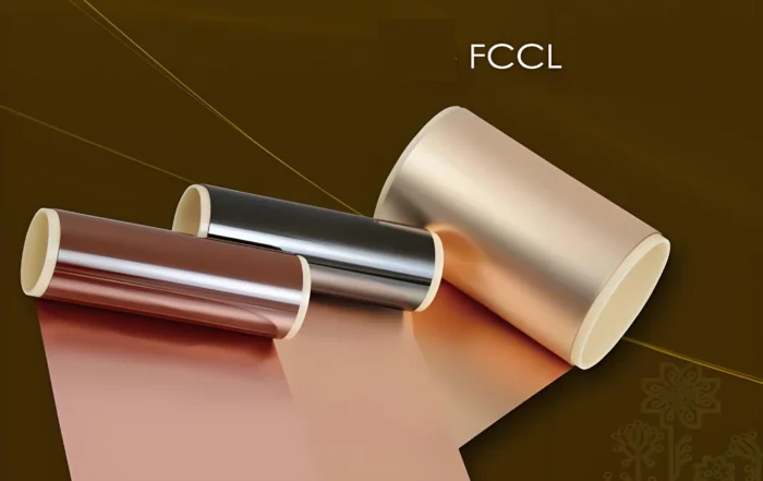
| Use adhesiveless laminates | Improves thermal reliability |
| Optimize lamination process | Strengthens interlayer bonding |
For high-reliability aerospace and medical electronics, adhesiveless laminates generally provide superior thermal stability and longer flex life compared with adhesive-based constructions.
Solder Joint and Pad Failure
Surface-mount solder joints behave very differently on flexible substrates than on rigid PCBs.
When the circuit bends, solder joints experience concentrated stress because solder is relatively rigid while the surrounding substrate remains flexible. This mismatch creates high strain around component pads.
Larger components—including connectors, transformers, shields, and BGAs—generate greater bending moments and therefore exhibit higher failure rates.
Major Causes
- Components located within flex regions
- Large or heavy packages
- Insufficient mechanical support
- Repeated vibration
- Thermal expansion mismatch
Design Recommendations
| Solution | Reliability Benefit |
|---|---|
| Place components in rigid sections | Eliminates bending stress |
| Add FR-4 or polyimide stiffeners | Supports solder joints |
| Increase pad anchoring | Reduces pad lifting |
| Use strain-relief routing | Distributes mechanical load |
Rigid-flex designs commonly incorporate FR-4 stiffeners beneath connector areas to protect solder joints during insertion and removal.
Coverlay Cracking
The coverlay serves as the flexible PCB equivalent of solder mask. It protects copper traces against moisture, abrasion, and contamination while maintaining flexibility.
However, repeated bending can initiate cracks at coverlay edges, particularly around narrow openings or sharp internal corners.
Causes
Stress naturally concentrates where geometry changes abruptly.
Design features that increase failure risk include:
- Sharp coverlay openings
- Narrow neck regions
- Small bend radii
- Abrupt trace transitions
Prevention
Modern flex PCB design emphasizes gradual stress distribution.
Recommended practices include:
- Larger bend radii
- Rounded coverlay openings
- Teardrop pad transitions
- Smooth copper geometry
- Uniform coverlay clearance
These techniques reduce peak stress while extending coverlay service life.
Material Selection Has a Major Impact on Reliability
Choosing appropriate materials often determines whether a flexible PCB survives thousands or millions of bending cycles.
| Material | Reliability Characteristics | Typical Applications |
|---|---|---|
| Rolled Annealed (RA) Copper | Excellent fatigue resistance | Dynamic flex |
| Electrodeposited (ED) Copper | Lower fatigue life | Static flex |
| Polyimide | High temperature resistance and flexibility | Most flexible PCBs |
| Adhesiveless Laminate | Superior thermal reliability | Medical, aerospace |
| FR-4 Stiffener | Mechanical reinforcement | Component mounting |
| Polyimide Stiffener | Lightweight reinforcement | Thin flexible assemblies |
Although RA copper and adhesiveless laminates increase manufacturing cost, they often reduce field failures enough to justify the investment in high-reliability products.
Design Guidelines for Improving Flex PCB Reliability
Successful flexible PCB design considers mechanical behavior from the earliest design stage rather than treating flexibility as an afterthought.
Several principles consistently improve reliability:
| Design Rule | Engineering Objective |
|---|---|
| Keep traces parallel to bend direction | Reduce tensile strain |
| Avoid vias inside bend regions | Prevent barrel cracking |
| Increase bend radius | Lower copper fatigue |
| Position components in rigid areas | Protect solder joints |
| Use RA copper for dynamic flex | Extend bending life |
| Bake boards before assembly | Prevent moisture-related failures |
| Add stiffeners beneath connectors | Reduce mechanical stress |
| Use teardrop pads and rounded corners | Eliminate stress concentration |
Following IPC-2223 recommendations throughout layout and manufacturing helps achieve longer operational life and fewer field failures.
Conclusion
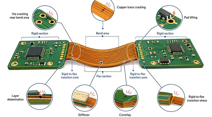
Flexible PCBs deliver exceptional advantages in compact, lightweight electronic systems, but their reliability depends heavily on sound mechanical design. Copper trace fatigue, via barrel cracking, delamination, solder joint failure, and coverlay cracking all originate from stress concentrations that engineers can largely prevent through thoughtful material selection and layout optimization.
Selecting rolled annealed copper, maintaining adequate bend radii, keeping vias and components away from flexible regions, using stiffeners where necessary, and controlling moisture before assembly significantly improve long-term durability. Combined with IPC design guidelines and robust manufacturing processes, these practices enable flexible circuits to withstand demanding environments in automotive, medical, aerospace, and industrial applications while maintaining reliable electrical performance.
References
- IPC-2223D, Sectional Design Standard for Flexible Printed Boards, IPC Association Connecting Electronics Industries.
- IPC-6013D, Qualification and Performance Specification for Flexible Printed Boards, IPC.
- IPC-9701A, Performance Test Methods and Qualification Requirements for Surface Mount Solder Attachments, IPC.
- NASA Electronic Parts and Packaging (NEPP) Program. Printed Wiring Board Reliability Studies. https://nepp.nasa.gov/
- J. H. Lau, Flexible Circuit Technology, McGraw-Hill.
- Harper, C. A., Electronic Materials and Processes Handbook, McGraw-Hill.
- DuPont Electronics & Industrial. Pyralux Flexible Circuit Materials Technical Data Sheets.
- DuPont. Kapton® Polyimide Film Technical Guide.