
Multilayer Flex PCB Stackup Design: How to Plan Layer Order & Build-Up from Customer Data
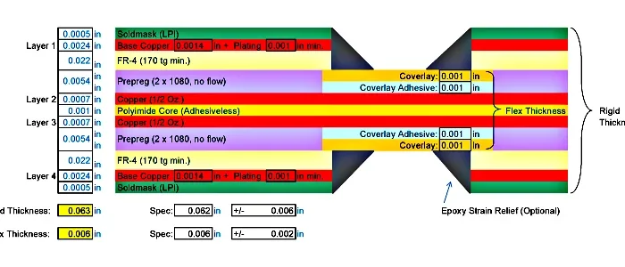


Therefore, multilayer flex PCB stackup design starts with customer data, not a standard layer template. Additionally, first, convert electrical, mechanical, and assembly requirements into constraints. Next, assign signal, power, and ground layers around bend zones. Meanwhile, calculate build-up thickness and confirm DFM with the fabricator before release.
.As a result, layer count is only one output. In practice, the real goal is a repeatable stack that meets impedance, bend life, thickness, and assembly needs.
Next, this guide follows a practical order: core terms, material choices, layer configuration, DFM and reliability checks, then FAQ. Consequently, that order helps cover both first-time stackup questions and long-tail searches such as 4-layer flex cross-section, rigid-flex transition thickness, and flex bend radius.
Core Terms in Multilayer Flex PCB Stackup Design
Moreover, a clear vocabulary prevents costly assumptions later. In particular, use these terms consistently in the stackup drawing and design review.
- Stackup: the ordered sequence of copper layers, dielectric cores, adhesives, coverlays, and reinforcements.
- Build-up: the total material construction and finished thickness from one outer surface to the other.
- Neutral axis: the plane in a bent flex where tensile and compressive strain are near zero. Place bend-sensitive copper close to it.
- Bend line: the axis around which the flex folds. Route traces perpendicular to this line in dynamic bends.
- Transition zone: the region where a flex cable meets a rigid board, stiffener, or connector. It is a common stress and return-path risk.
- Coverlay: a protective polyimide film with adhesive that covers outer copper. It affects bend life and impedance.
- Stiffener: local reinforcement, usually FR4 or PI, placed outside the bend zone to support connectors or components.
- Adhesive vs adhesiveless: adhesive-based laminates use a bonding layer; adhesiveless laminates are thinner and more dimensionally stable.
What Multilayer Flex PCB Stackup Design Must Solve
However, multilayer flex PCB stackup design balances four needs: signal integrity, mechanical bending, thermal path, and manufacturability. Therefore, a stack that works in a flat rigid board may fail in a dynamic flex bend. Therefore, the layer order must follow the mechanical layout, not just the netlist.
Additionally, three inputs drive every decision: the schematic and netlist, the mechanical envelope, and the assembly process. Meanwhile, missing data creates guesswork. For example, a good stackup record shows why each layer, material, and thickness exists.
Step 1: Convert Customer Data into Stackup Constraints
In addition, before drawing a stack, turn the customer package into a written constraint list. As a result, use the table below as an intake checklist. In practice, ask for missing data in one round, not five.
| Customer data | Question to ask | Stackup impact |
|---|---|---|
| Schematic and netlist | Which nets are high speed, power, or sensitive? | Layer count and ground assignment |
| Impedance target | What single-ended or differential value is required? | Dielectric thickness and line geometry |
| Bend requirement | Static or dynamic? What radius and cycle count? | Copper type, layer symmetry, coverlay |
| Current and thermal load | What is the maximum current and ambient temperature? | Copper weight, thermal path, plane design |
| Connector and components | Where are stiffeners, pads, and assembly sides? | Reinforcement location and coverlay openings |
| Environment | Humidity, chemicals, vibration, or flex cycling? | Material grade and surface finish |
| Volume and cost | Prototype, low volume, or mass production? | Adhesive vs adhesiveless, panel utilization |
Next, also capture panel size, test method, and acceptance criteria. Consequently, these details affect tooling and yield. Therefore, a stackup without test data is incomplete.
Step 2: Select a 2-Layer, Multilayer, or Rigid-Flex Architecture
Moreover, use architecture selection to remove weak options early. In particular, two-layer flex suits simple routing and tight bends. However, multilayer flex adds ground planes and dense routing. Therefore, rigid-flex adds support, but it also adds transition zones and cost.
| Architecture | Typical layer range | Best for | Watch-outs |
|---|---|---|---|
| 2-layer flex | 1-2 copper layers | Simple circuits and dynamic bends | Limited shielding and routing |
| Multilayer flex | 3-8 copper layers common; higher on request | Controlled impedance and dense I/O | Bend symmetry and thickness |
| Rigid-flex | Mixed flex and rigid layers | Connector-heavy and board-to-board designs | Stress at the transition zone |
Additionally, treat layer counts above the common range as a custom engineering review. Meanwhile, do not promise them without a fabricator check.
Step 3: Select Materials for the Flex Build-Up
For example, material choice sets the limits for bend life, impedance, and thickness. In addition, start with supplier datasheets, not generic estimates. As a result, the table below gives typical starting values for planning; the fabricator must confirm final values.
| Layer | Typical starting value | Design note |
|---|---|---|
| Coverlay | 25 µm PI plus 12-25 µm adhesive | Check openings and bend zone |
| Copper | 17 µm (0.5 oz) or 35 µm (1 oz) | Use RA copper for dynamic bends |
| PI core | 25 µm or 50 µm | Use supplier data, not estimates |
| Adhesive | 20-25 µm | Squeeze-out affects impedance |
| PSA | 25-50 µm | For bonding, not in the bend |
| Stiffener | 0.2-1.0 mm FR4 or PI | Keep outside the bend zone |
In practice, compare adhesive and adhesiveless options early. Next, adhesiveless builds are thinner and more stable. Consequently, adhesive builds can reduce cost for less demanding bends. Moreover, for dynamic bends, use rolled annealed copper. In particular, for static or low-bend areas, electrodeposited copper may meet cost and fine-line needs.
Step 4: Plan Layer Order and Signal Assignment
Layer order is where most stackup errors appear. Use these rules as a starting point, then verify with simulation and DFM.
1. Place a continuous ground plane next to every high-speed signal layer. The return current needs a short path.
2. Pair power and ground planes. This lowers loop inductance and adds distributed capacitance.
3. Balance copper distribution around the neutral axis. Unbalanced copper can warp the flex and reduce bend life.
4. Keep bend-critical traces away from coverlay openings and stiffener edges. These are stress concentrators.
5. Route bend-zone traces perpendicular to the bend line. Long parallel traces see more strain.
6. Use crosshatch copper for large static planes in bend areas. It improves flexibility, but model the electrical effect.
7. Place reinforcement outside the bend zone. Choose material and thickness from the flex reinforcement guide.
Also decide where shielding belongs. Apply an EMI shielding method only after the ground scheme and layer order are stable. Shielding cannot fix a broken return path.
Step 5: Calculate Build-Up Thickness and Tolerance
Build-up thickness is a sum, not a guess. Add every layer from the outer surface to the opposite surface. Include adhesive, coverlay, PSA, stiffener, and shielding. Then compare the nominal value with the tolerance stack.
Total thickness = coverlay + adhesive + copper + core + adhesive + copper + … + stiffener + shielding.
Write the calculation into the stackup drawing. Mark nominal and tolerance for each material. If the result is close to the bend-radius limit, reduce thickness or change the layer order before release.
Example only: a four-copper-layer flex with 25 µm coverlays, 17 µm copper, and 25 µm PI cores may land near 0.24 mm before stiffener. Confirm the final drawing with a fabricator.
Step 6: Protect the Bend Zone in the Layer Plan
Bending performance is a stackup property. It comes from copper type, layer symmetry, thickness, and trace direction. A flexible PCB with balanced copper and thin dielectrics usually bends better than an unbalanced thick stack.
FPC bending resistance depends on strain at the copper. Place conductors near the neutral axis where possible. Use rolled annealed copper for dynamic bends. Use electrodeposited copper for static or low-bend areas when cost matters.
Keep stiffeners and coverlay openings out of the bend. Add teardrops and anchor pads. Review FPCB pad cracking prevention before release. Small pad details often decide field life.
Step 7: Control Impedance in a Flexible Dielectric
Impedance in flex is not a copy of a rigid stack. The dielectric is thinner, the coverlay changes the field, and adhesive thickness varies. Start with the target, then solve for line width and dielectric height.
Use a solid reference plane under high-speed traces. Get Dk and Df values from the laminate supplier at the relevant frequency. Include coverlay and adhesive in the field model. Also define the measurement coupon and tolerance.
In addition, check the transition from flex to stiffener or rigid board. The reference plane must stay continuous. A split return path can ruin an otherwise good stack.
Step 8: Close the Loop with DFM and Reliability Checks
Run a DFM review before quotation, not after tooling. The checklist should match the actual stack.
- Minimum bend radius vs total thickness and copper type
- Layer symmetry and copper balance
- Coverlay and stiffener keepouts
- Via and pad anchoring in bend zones
- Impedance coupon and test method
- Panel utilization and assembly panel
- FPCB heat dissipation path for power components
- Shielding ground connection
Write each decision into the FPC design file with a reason. This makes the stack auditable and easier to transfer between engineers.
Typical Flex Stackup Cross-Sections
The examples below are conceptual cross-sections from top to bottom. They label nominal materials and thicknesses for planning. They are not released constructions. The fabricator must confirm copper weights, adhesive flow, coverlay openings, and tolerances before tooling.
4-Layer Flex Cross-Section
| Layer (top to bottom) | Material/function | Nominal thickness |
|---|---|---|
| Coverlay | PI film + adhesive | 25 µm PI + 25 µm adhesive |
| L1 copper | Signal, 0.5 oz RA copper | 17 µm |
| Core | PI | 25 µm |
| L2 copper | Ground plane | 17 µm |
| Bonding layer | Adhesive | 25 µm |
| Core | PI | 25 µm |
| L3 copper | Power plane | 17 µm |
| Core | PI | 25 µm |
| L4 copper | Signal, 0.5 oz RA copper | 17 µm |
| Coverlay | PI film + adhesive | 25 µm PI + 25 µm adhesive |
Electrical order: signal/ground/power/signal. The two inner planes support impedance and current. Keep stiffeners outside the bend.
6-Layer Flex Cross-Section
| Layer (top to bottom) | Material/function | Nominal thickness |
|---|---|---|
| Coverlay | PI film + adhesive | 25 µm PI + 25 µm adhesive |
| L1 copper | Signal | 17 µm |
| Core | PI | 25 µm |
| L2 copper | Ground | 17 µm |
| Bonding layer | Adhesive | 25 µm |
| Core | PI | 25 µm |
| L3 copper | Signal | 17 µm |
| Core | PI | 25 µm |
| L4 copper | Power | 17 µm |
| Bonding layer | Adhesive | 25 µm |
| Core | PI | 25 µm |
| L5 copper | Ground | 17 µm |
| Core | PI | 25 µm |
| L6 copper | Signal | 17 µm |
| Coverlay | PI film + adhesive | 25 µm PI + 25 µm adhesive |
Electrical order: signal / ground / signal / power / ground / signal. This adds routing room and a second ground reference. Check symmetry around the neutral axis.
8-Layer Flex Cross-Section
| Layer (top to bottom) | Material/function | Nominal thickness |
|---|---|---|
| Coverlay | PI film + adhesive | 25 µm PI + 25 µm adhesive |
| L1 copper | Signal | 17 µm |
| Core | PI | 25 µm |
| L2 copper | Ground | 17 µm |
| Bonding layer | Adhesive | 25 µm |
| Core | PI | 25 µm |
| L3 copper | Signal | 17 µm |
| Core | PI | 25 µm |
| L4 copper | Power | 17 µm |
| Bonding layer | Adhesive | 25 µm |
| Core | PI | 25 µm |
| L5 copper | Ground | 17 µm |
| Core | PI | 25 µm |
| L6 copper | Signal | 17 µm |
| Bonding layer | Adhesive | 25 µm |
| Core | PI | 25 µm |
| L7 copper | Ground | 17 µm |
| Core | PI | 25 µm |
| L8 copper | Signal | 17 µm |
| Coverlay | PI film + adhesive | 25 µm PI + 25 µm adhesive |
Electrical order: signal / ground / signal / power / ground / signal / ground / signal. An 8-layer flex needs a careful symmetry check. More layers can improve shielding and routing, but they also raise thickness and reduce bend life.
Rigid-Flex Transition Zone Cross-Section
A rigid-flex transition is not a simple layer count change. It is a controlled stress and return-path region. The example below shows one side of the transition. The rigid side may include additional prepreg and FR4 layers.
| Region (top to bottom) | Material/function | Nominal thickness |
|---|---|---|
| Rigid coverlay / solder mask | Rigid board surface | Per rigid build |
| Rigid prepreg + FR4 | Rigid support | Per rigid build |
| Transition adhesive | Bonding layer | 25-50 µm |
| Flex coverlay | PI film + adhesive | 25 µm PI + 25 µm adhesive |
| Flex L1 copper | Signal | 17 µm |
| Flex core | PI | 25 µm |
| Flex L2 copper | Ground | 17 µm |
| Flex bonding layer | Adhesive | 25 µm |
| Flex core | PI | 25 µm |
| Flex L3 copper | Power | 17 µm |
| Flex core | PI | 25 µm |
| Flex L4 copper | Signal | 17 µm |
| Flex coverlay | PI film + adhesive | 25 µm PI + 25 µm adhesive |
| Stiffener (outside bend) | FR4 or PI | 0.2-1.0 mm |
Mark the transition zone on the drawing. Keep the ground reference continuous across the transition. Avoid placing vias or pad edges at the transition boundary. Use a gradual stiffness change where possible.
FAQ
How many layers can a multilayer flex PCB stackup design support?
Most multilayer flex designs use 3 to 8 copper layers. Counts above 8 to 10 are possible, but they need a custom review for bend life, thickness, and yield. The right count comes from routing, impedance, and shielding needs, not a target number.
What customer data is needed before stackup design?
You need the schematic and netlist, impedance targets, bend radius and cycle count, current and thermal load, connector and stiffener locations, assembly method, environment, and volume. Also request panel size, test method, and acceptance criteria. Missing data should be closed before layer order is fixed.
Which materials are common in a flex stackup?
Common materials include polyimide core and coverlay, rolled annealed or electrodeposited copper, acrylic or epoxy adhesive, PSA for bonding, and FR4 or PI stiffeners. Adhesiveless laminates are thinner and more stable; adhesive builds can be lower cost for less demanding bends.
Should I use RA or ED copper in a flex stackup?
Use rolled annealed copper for dynamic bend zones because it resists fatigue better. Use electrodeposited copper for static or low-bend areas when cost and fine-line needs favor it. The final choice depends on bend radius, copper thickness, and layer symmetry.
How do I calculate flex stackup thickness?
Add every material layer from one outer surface to the other: coverlay, adhesive, copper, PI core, PSA, stiffener, and shielding. Use supplier datasheets for nominal values, then add tolerance. Confirm the result with a fabricator drawing before release.
How does bend radius affect the stackup?
Bend radius sets the allowable strain in the copper. A tighter radius usually requires thinner dielectrics, RA copper, balanced layer construction, and careful trace direction. If the calculated strain is too high, change the stack or increase the bend radius before release.
What drives cost in a multilayer flex stackup?
Cost is driven by layer count, material choice, adhesiveless vs adhesive construction, stiffener and shielding requirements, panel utilization, and test method. Higher layer counts and tight tolerances add process steps. A DFM review before quotation helps avoid cost surprises.
Related Posts
- FPC Laminate Design: Stackup & Neutral Axis Guide 2026 — Related article
- Flexible PCB: Features, Design Guide & Applications — Related article
- Boosting PCB and FPCB Heat Dissipation — Related article
- EMI Shielding Method for FPC and Flex Circuits Guide — Related article
- FPC Bending Resistance: Design Guide for Flex Circuits — Related article