
FPC Bending Resistance: How to Design FPCs for Good Resistance to Bend
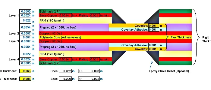


Therefore, good FPC bending resistance comes from three decisions. Additionally, first, match the design to static or dynamic bending. Next, keep the flex PCB bend radius design large enough for the stack thickness and layer count. Finally, place copper, coverlay, and stiffeners so strain spreads over a wide area. Meanwhile, materials and process then support those choices.
Static Bending or Dynamic Bending? Start Here
For example, the first decision is the duty cycle of the bend. In addition, static bending happens once or a few times, during installation or assembly. As a result, typical cases are internal links in smartphones, camera modules, laptops, and display assemblies. After assembly, the flex stays still.
In practice, dynamic bending repeats throughout the product life. Next, flip phone hinges, foldable displays, robotic arm wiring, automotive steering sensors, medical wearables, and vibration-exposed industrial sensors all belong here. FPC dynamic bending therefore changes the target. Consequently, the aim moves from no crack on installation to fatigue life.
Moreover, industry reliability practice treats a static bend design as adequate when it survives fewer than 100 cycles without electrical discontinuity. In particular, dynamic designs need far more.
| Design point | Static bending | Dynamic bending |
|---|---|---|
| Bend duty | Fewer than 100 cycles | Repeated, up to 10⁵–10⁷ with rolled annealed copper |
| Typical inner radius | 1×–3× total thickness | ≥10× total thickness; higher for long life |
| Copper foil | RA or ED | RA preferred |
| Copper thickness in bend zone | 1 oz or thinner; 0.5 oz common | 0.5 oz or thinner; 12–18 μm where possible |
| Layer count | Single-layer or simple multilayer | Single-layer or thin multilayer; keep copper near neutral axis |
| Main risk | Copper cracking and delamination during forming | Fatigue micro-cracks that grow into opens |
| Design aim | No cracks on installation | Fatigue life over product life |
Flex PCB Bend Radius Design: The Rule That Sets Everything Else
However, bend radius is the inner radius the flex wraps around. Therefore, it sets the strain the copper must survive. Additionally, surface strain rises with stack thickness and falls as the radius grows: strain ≈ total thickness ÷ (2 × bend radius).
For example, a 0.20 mm stack on a 2 mm radius carries about twice the surface strain of a 0.10 mm stack on the same radius. Therefore, thin cores and thin copper pay off quickly.
Meanwhile, common starting points in design reviews are:
- Static installation bend: 1× to 3× total thickness.
- Occasional rework bend: about 5× total thickness.
- FPC dynamic bending: 10× total thickness or more, with higher ratios for very long life.
For example, the design rule can be written as a strain estimate. In addition, for a stack bent to inner radius R, the outer copper surface strain is approximately ε ≈ T_total ÷ (2 × R). As a result, rearranged, the minimum radius for an allowable strain is R_min = T_total ÷ (2 × ε_allow). In practice, this is why layer count matters: every added copper and dielectric layer increases T_total.
| Total stack thickness | Layer count example | Static starting radius (1×–3×T) | Dynamic starting radius (≥10×T) |
|---|---|---|---|
| 0.10 mm | 1-layer, thin PI + 0.5 oz Cu | 0.10–0.30 mm | ≥1.0 mm |
| 0.15 mm | 1-layer with coverlay | 0.15–0.45 mm | ≥1.5 mm |
| 0.20 mm | 2-layer | 0.20–0.60 mm | ≥2.0 mm |
| 0.30 mm | 4-layer | 0.30–0.90 mm | ≥3.0 mm |
| 0.40 mm | 4–6-layer or stiffened | 0.40–1.20 mm | ≥4.0 mm |
Next, worked example: a 0.15 mm stack with an allowable copper strain of 1.0% (0.010) needs R_min = 0.15 ÷ (2 × 0.010) = 7.5 mm. Consequently, a 0.30 mm four-layer stack at the same strain target needs 15 mm. Moreover, if the application allows 2.5% strain, the same 0.30 mm stack can use 6 mm, but fatigue life will be shorter. In particular, this connects thickness, layer count, radius, and strain in one calculation.
However, measure the radius on the inside of the fold, and prefer a gradual curve over a crease. Therefore, also keep the bend line away from the part edge.
Copper Fatigue, Work Hardening and Bending Strain: Why the Rules Exist
When an FPC bends, the outer copper is pulled in tension, and the inner copper is compressed. The neutral axis sits between them. The farther copper sits from the neutral axis, the higher the tensile strain. Repeated bending causes dislocation motion inside the copper grains. The copper work-hardens, local stress rises, and micro-cracks start at grain boundaries or at etch edges. Once a micro-crack crosses the trace, the circuit opens.
Rolled annealed (RA) copper has elongated grains that resist fatigue crack growth better than electrolytic (ED) copper. ED copper has columnar grains and often cracks earlier under the same strain. Work hardening also explains why a sharp crease is worse than a gradual arc: the crease concentrates strain into a short length, so the local copper reaches its fatigue limit after fewer cycles. The design rules in this article follow directly from that mechanism: keep total thickness low, choose RA copper for dynamic bends, route traces perpendicular to the bend, remove vias and stiff features, and open the coverlay so the stack flexes over a longer arc.
Copper Foil, Thickness and Trace Angle: Quantifying the Bend Zone
| Variable | Recommended for dynamic bend | Effect on bend life | Quantitative guide |
|---|---|---|---|
| Foil type | Rolled annealed (RA) | RA delays fatigue cracking; ED can fail earlier at the same strain | RA flex circuits often reach 10⁵–10⁷ cycles under optimized strain; ED commonly fails at lower cycle counts |
| Copper thickness | 12–18 μm (0.5 oz or thinner) | Thinner copper sits closer to the neutral axis and lowers strain | Halving copper thickness roughly halves the copper contribution to surface strain at the same radius |
| Trace direction vs bend axis | Perpendicular (90°) | Strain acts across trace width instead of along trace length | Keep traces within 30° of perpendicular; parallel traces carry strain over the full bend length |
| Trace width and spacing | Wider spacing and curved transitions | Reduces local strain concentration | Avoid tight bundles in the bend zone; spread traces and use teardrops at pads |
Minimum Bend Radius Formula and Worked Examples
Use the strain estimate ε ≈ T_total ÷ (2 × R), where T_total is the full stack thickness including copper, PI, adhesive, and coverlay. Rearranged for design: R_min = T_total ÷ (2 × ε_allow). The allowable strain depends on the cycle target. A conservative long-life dynamic target may use 0.5%–1.0%; a static installation bend may allow 2.0%–3.0%.
Example 1: single-layer, T_total = 0.12 mm, ε_allow = 1.0% (0.010). R_min = 0.12 ÷ (2 × 0.010) = 6.0 mm.
Example 2: four-layer, T_total = 0.30 mm, ε_allow = 1.0% (0.010). R_min = 0.30 ÷ (2 × 0.010) = 15.0 mm. If the design uses a 6 mm radius, the estimated strain is 0.30 ÷ (2 × 6) = 2.5%, so expect shorter fatigue life.
Example 3: static bend, T_total = 0.20 mm, ε_allow = 2.5% (0.025). R_min = 0.20 ÷ (2 × 0.025) = 4.0 mm.
These examples show why layer count and copper thickness must be in the bend-radius discussion. Adding layers raises T_total and pushes R_min up unless the strain allowance is relaxed.
Copper Foil and Dielectric Choice for Bend Life
Polyimide (PI) is still the standard base film. It brings thermal stability, flexibility, and mechanical durability. For dynamic designs, thinner cores work better, commonly 0.5 mil (12.5 μm) or 1 mil (25 μm). A thinner substrate reduces the neutral axis distance and lowers tensile strain in the copper.
Copper foil determines fatigue behavior. Rolled annealed (RA) copper flex circuits can endure 10⁵–10⁷ bending cycles under optimized conditions. Electrolytic copper often fails at much lower cycle counts at the same strain level. The gap comes from grain morphology and from how strain spreads across the trace.
In addition, keep the copper thin inside the bend zone. Specify rolled copper foil for FPC builds that flex for the whole product life. In multilayer builds, place the copper layer near the neutral axis. Every flexible PCB that bends continuously deserves this review at the stack-up stage.
Routing, Coverlay and Stress Relief Rules
Most bend failures start where strain concentrates. Route conductors across the bend axis, not along it. Then remove every stiff feature from the bend zone.
Rules that apply to almost every design:
- Route traces perpendicular to the bend axis.
- Round trace transitions and add teardrops at pads.
- Keep vias, plated holes, and solder pads out of the bend area.
- Widen the bend zone and avoid 90° steps in the outline.
- Cross-hatch or open the coverlay over the bend to cut stiffness.
- Round every coverlay window, because a sharp corner becomes a tear start.
- Place stiffeners and component areas outside the bend zone only.
- Remove soldermask from the bend zone or use a coverlay opening; soldermask cracks can initiate tears.
- Define a no-route zone around the bend; no copper pour, plane, or component keep-out should cross it.
- Keep trace width and spacing uniform through the bend; avoid tight bundles.
Rigid-to-flex transitions need the same care. The same logic applies to rigid-flex PCB technology: put the transition line outside the highest-strain region, and treat the rigid-flex PCB bond area as a stiff zone.
A Pre-Release Checklist for FPC Bending Resistance
Run this list before the design leaves engineering:
- Bend type recorded: static or dynamic, with a cycle target.
- Minimum bend radius calculated with R_min = T_total ÷ (2 × ε_allow), not guessed.
- Copper type and foil thickness confirmed for the bend zone.
- Trace direction within 30° of perpendicular to the bend axis.
- Trace width and spacing reviewed; no tight bundle in the bend zone.
- No vias, pads, plated holes, or component keep-out in the bend zone.
- Solder mask removed or not used in the bend zone; coverlay opened or cross-hatched.
- Coverlay window corners rounded.
- Stiffeners and reinforcement edges kept outside the bend zone.
- No copper pour or plane in the bend zone unless cross-hatched.
- Bend line at least one part thickness from the outline edge.
- Stack drawing shows layer order, total thickness, coverlay openings, and no-route zone.
- Fabrication drawing shows the bend axis and radius target.
The same list works for simple flexible circuit boards and for multilayer stacks. Add the bend axis and the radius target to the fabrication drawing, so the shop builds what you modeled.
Design, Material, Manufacturing and Assembly Boundaries
Bending resistance is not a layout-only problem. The designer owns bend axis, radius target, cycle target, stack thickness, and keep-out zones. The material engineer owns PI thickness, adhesive, copper foil type (RA or ED), copper thickness, and coverlay material. However, the fabricator owns etch quality, coverlay registration, surface finish, stiffener bond, and panel handling. Assembly owns bend tooling radius, bend speed, cable routing, and strain relief. A design review should record these boundaries on one drawing. Otherwise, a layout that looks good can fail because the shop etched a thicker copper, the assembly bent on a sharp tool, or the coverlay window was registered off-center. Define the bend zone as a shared process control, not just a geometry note.
Common Mistakes and Before/After Fixes
| Common mistake | Why it fails | Before → after correction |
|---|---|---|
| Traces run parallel to bend line | Strain accumulates along the full trace length | Reroute perpendicular to bend axis; spread traces |
| Via or pad inside bend zone | Stress concentration starts a crack | Move via/pad outside bend; add teardrop near transition |
| Solid coverlay over bend | Adds stiffness and pushes strain into copper | Open or cross-hatch coverlay; round window corners |
| Sharp outline step at bend | Creates a tear start and uneven strain | Smooth outline; widen bend zone |
| Stiffener crosses bend | Makes a rigid-to-flex transition inside the strain zone | Move stiffener edge outside bend; extend transition length |
| Copper too thick for radius | Raises strain at the same radius | Reduce Cu to 0.5 oz or thinner; increase radius |
| Wrong foil for dynamic life | ED copper fatigues earlier than RA | Switch to RA copper for dynamic bend |
| Soldermask in bend zone | Cracks and initiates coverlay tears | Remove soldermask; use coverlay window |
Failure Modes and How to Verify Bend Life
Three failure modes dominate. Copper micro-cracks start on the outer surface and grow into opens. Delamination appears between the polyimide and the copper or adhesive. Substrate tears begin at a sharp coverlay or stiffener edge.
Verification follows the same order. Run a cyclic bend test at the specified radius and monitor continuity during the run. Then check a cross-section for copper cracking and layer separation. Add these checks to your PCB testing methods list, and log the cycle count with the test radius.
Suppliers who build high-reliability flexible circuits for high-end applications usually ask for three items: bend radius, cycle target, and bend axis. Answer them early, and the first article is far easier to approve. Any open point on stack-up or tolerance can go through the PCB Manufacturing FAQ.
FAQ
What is the minimum bend radius for an FPC?
The minimum bend radius depends on total stack thickness and on bend duty. A working estimate is strain ≈ total thickness ÷ (2 × bend radius), or R_min = T_total ÷ (2 × ε_allow). Static installation bends often sit at 1× to 3× the total thickness. FPC dynamic bending usually needs 10× or more. Thin polyimide cores with rolled annealed copper make the smaller radii practical.
Should FPC traces run parallel or perpendicular to the bend line?
Perpendicular. Traces that cross the bend axis see strain over a short length. Traces that run along the fold carry strain over their full length, so they crack first. If routing forces a parallel run, widen the bend zone, spread the traces, and keep them away from the outer surfaces of the stack.
Why open the coverlay in the bend area?
The coverlay adds thickness and stiffness to the stack. A solid coverlay layer pushes more strain into the copper during each bend. An open or cross-hatched coverlay lowers that stiffness, so the copper flexes over a longer arc. Round every window edge, because a sharp corner becomes a tear start point.
How do copper foil type and trace angle affect FPC bending resistance?
Rolled annealed copper has elongated grains that resist fatigue better than electrolytic copper, so RA is preferred for dynamic bends. Trace angle matters because perpendicular traces see strain across a short width, while parallel traces carry strain along their full length. Keep traces within 30° of perpendicular to the bend axis, reduce copper thickness in the bend zone, and increase radius until the calculated strain matches the cycle target.
Related Posts
- Rolled Copper Foil for FPC Optimization — Related article
- Flexible PCB: Features, Design Guide & Applications — Related article
- PCB Testing Methods: 8 Techniques for Quality Assurance — Related article
- AI-Driven Optimization of Flexible Circuit Boards Production — Related article
- Adhesive-Free FCCL Substrates vs Adhesive-Based FCCL — Related article