Advantages and disadvantages of flex PCB

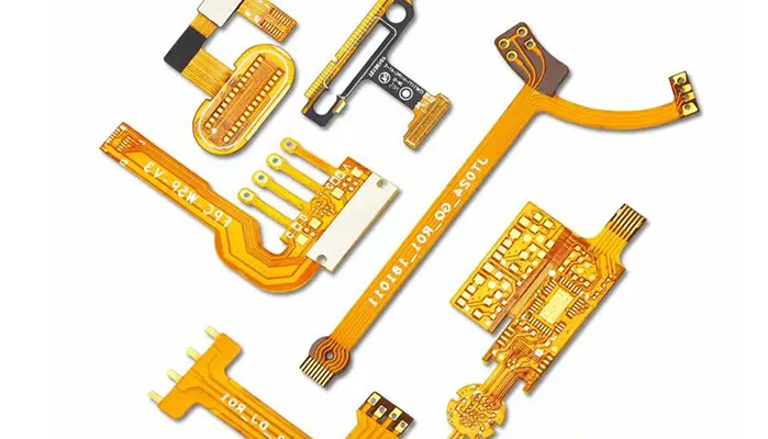
Flexible Printed Circuits (FPCs), often referred to as flex PCBs, are widely used in modern electronics where space, weight, and mechanical adaptability matter. However, their adoption is frequently driven by assumptions rather than system-level engineering analysis.
This article takes a design-centric perspective: where flex PCBs genuinely improve product performance, and where they introduce hidden risks that engineers often underestimate.
Why Flex PCB Is Not Just a Miniature Version of Rigid PCB
A common design misconception is treating flex PCB as a “thin, bendable rigid PCB.” In reality, flex circuits operate under fundamentally different physical constraints.
Rigid PCBs rely on dimensional stability, copper rigidity, and controlled thermal expansion in a static geometry. Flex PCBs, by contrast, must survive cyclic mechanical strain, dynamic bending radius limitations, and complex multilayer stress interactions.
Key engineering distinction
| Aspect | Rigid PCB | Flex PCB |
|---|---|---|
| Primary constraint | Electrical routing density | Mechanical strain + bend reliability |
| Failure mode | Solder fatigue, delamination | Trace cracking, coverlay lift |
| Design freedom | High planar density | 3D geometric freedom |
| Manufacturing tolerance | Moderate | Very tight (layer alignment, adhesive control) |
Flex PCB is therefore not “better”—it is a context-dependent engineering trade-off material system.
The Real Advantages of Flex PCB (Beyond Marketing Claims)
1. 3D Electronic Packaging Freedom
Flex circuits enable true three-dimensional routing of interconnects. Instead of being constrained to planar board stacking, engineers can integrate electronics directly into mechanical structures such as hinges, curved surfaces, and folding assemblies.
This reduces reliance on rigid board segmentation and allows enclosure-driven design to shift toward electronics-driven mechanical architecture.
Typical impact:
- Reduced enclosure volume
- Higher integration density
- Simplified electromechanical co-design
In foldable smartphones, for example, flex interconnects are the enabling backbone of the hinge system rather than a peripheral component.
2. Connector Elimination = Reliability Gain
One of the most underestimated advantages of flex circuits is the ease of connector removal.
Connectors are among the components with the highest failure rates in electronic assemblies, primarily due to fretting corrosion, vibration-induced loosening, and insertion wear. Industry reliability studies consistently show that connector-related failures contribute significantly to field returns in harsh environments.
Flex circuits replace:
- Board-to-board connectors
- Wire harnesses
- Solder-heavy interconnect paths
This results in:
- Fewer discrete failure points
- Lower assembly variability
- Reduced human assembly error rate
In automotive and aerospace systems, this shift is often more important than cost savings.
3. Extreme Space Optimization
Flex PCBs enable vertical and folded stacking architectures that rigid boards cannot achieve efficiently.
This is especially relevant in:
- Wearables (smart watches, biosensors)
- Medical devices (catheters, implants)
- Foldable consumer electronics
By eliminating rigid interconnect constraints, designers can reduce overall product footprint significantly.
A simplified comparison:
| Design Approach | Volume Efficiency |
|---|---|
| Rigid PCB + cables | Low |
| Rigid PCB + connectors | Medium |
| Flex PCB integrated assembly | High |
4. Dynamic Mechanical Stability
Flex circuits outperform rigid assemblies in vibration and flexing environments because they distribute strain across a continuous substrate rather than discrete solder joints.
This leads to:
- Lower solder joint fatigue
- Improved vibration endurance
- Better thermal cycling resilience in moving assemblies
Applications include:
- Automotive dashboards
- Aerospace control surfaces
- Industrial robotic joints
The key mechanism is strain distribution: flex substrates reduce localized stress concentration that typically leads to micro-cracking in rigid PCBs.
5. System-Level Weight Reduction
While individual FPCs are lightweight, the real benefit is at system level: elimination of cables, connectors, and support brackets.
In aerospace systems, even small reductions in harness mass translate into significant fuel efficiency gains over time. In portable devices, weight reduction directly improves usability and ergonomics.
Hidden Disadvantages of Flex PCB (What Manufacturers Don’t Emphasize)
Despite their advantages, flex circuits introduce engineering complexity that is often underestimated in early design phases.
1. High Engineering and Prototype Cost
Flex PCB materials—typically polyimide-based laminates—are significantly more expensive than FR-4 substrates. Additionally, adhesive systems, coverlays, and controlled impedance stack-ups increase material and process costs.
Cost drivers include:
- Specialty base films (polyimide)
- Adhesive systems (acrylic/epoxy variants)
- Precision lamination processes
- Lower panel utilization efficiency
A simplified cost trend comparison:
| Factor | Rigid PCB | Flex PCB |
|---|---|---|
| Material cost | Low | High |
| Prototype iteration cost | Moderate | High |
| Yield sensitivity | Moderate | High |
Cost does not scale linearly—complex geometries disproportionately increase expense.
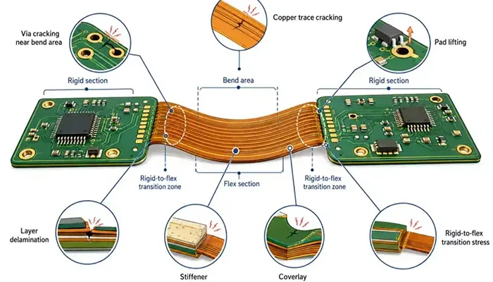
2. Mechanical Fragility in Real Assembly
Flex circuits are highly sensitive to handling damage before final integration.
Common failure risks:
- Micro-cracks in copper traces due to over-bending
- Tears during assembly handling
- Localized stress at bend transition zones
A critical design parameter is the minimum bend radius, typically defined as:
R ≥ 10 × thickness (dynamic flex applications often require higher safety margins)
Operator handling variability can also significantly affect yield, especially in manual assembly environments.
3. Design Restrictions That Reduce Density
Unlike rigid PCBs, flex circuits impose strict layout constraints.
Key limitations:
- No components in bending zones
- Restricted routing near bend edges
- Limited ability to increase via density in flexible regions
This often leads to a reduced effective routing area, even if the physical outline appears compact.
In practice, engineers frequently discover that “space saving” is partially offset by routing inefficiency in constrained zones.
4. Complex Stack-Up Engineering
Flex PCB stack-ups are significantly more sensitive than rigid designs due to multi-material interaction effects.
Key technical challenges include:
- Copper-to-polyimide adhesion stability
- Adhesive creep under thermal cycling
- Layer-to-layer registration accuracy in multilayer flex
Even small variations in lamination pressure or curing profile can lead to:
- Delamination
- Impedance drift
- Mechanical warping
This makes process control far more critical than in standard FR-4 production.
5. Repairability Problem
Once laminated and assembled, flex circuits are extremely difficult to rework.
Challenges include:
- Coverlay removal without damaging traces
- Limited re-soldering tolerance
- High risk of irreversible damage during field repair
Unlike rigid boards, where components can often be replaced, flex PCBs frequently require full assembly replacement in case of failure.
This significantly impacts total lifecycle cost in serviceable products.
Engineering Decision Perspective: When Should You Use Flex PCB?
The decision is not about capability—it is about system constraints.
| Use Flex PCB when… | Avoid Flex PCB when… |
|---|---|
| 3D packaging is required | Flat PCB layout is sufficient |
| Connector failure risk is critical | Low-cost design dominates |
| Weight reduction is system-critical | Repairability is required |
| Dynamic motion exists | Static electronics only |
| Space is highly constrained | Volume is available |
The Most Important Engineering Truth: Flex PCB Is a Mechanical System, Not Just an Electrical One
One of the most persistent design errors in flex circuit development is treating it as a purely electrical routing medium. In practice, a flexible printed circuit behaves much closer to a mechanical fatigue structure embedded with conductors.
The electrical schematic may be correct, but field failures often originate from mechanical stress accumulation over time.
Flex PCB behaves like a dynamic mechanical component
Unlike rigid FR-4 boards, flex circuits continuously experience:
- Tensile strain on outer bend radius
- Compressive strain on inner radius
- Interlayer shear stress in multilayer constructions
- Creep and relaxation effects in adhesive systems
These are mechanical phenomena, not electrical ones. The circuit “works” electrically until copper fatigue propagation reaches a critical threshold, at which point open circuits appear suddenly.
Electrical failure is often mechanical in origin
Field failure analysis consistently shows that many “electrical failures” (open circuits, intermittent signals, impedance drift) originate from:
- Repeated bending cycles beyond design limits
- Improper neutral axis placement
- Copper work-hardening and micro-crack propagation
- Adhesive delamination causing trace strain concentration
This is why flex PCB reliability cannot be evaluated using only schematic review or signal integrity simulation.
Neutral axis concept determines long-term reliability
A key engineering principle in flex design is the neutral axis—the layer within the stack-up where tensile and compressive strain is theoretically zero during bending.
If copper is placed away from this axis, it experiences cyclic strain during every bend event.
A simplified relationship is:
Strain ∝ (Distance from neutral axis) / Bend radius
This means:
- Closer copper placement to neutral axis → higher fatigue life
- Off-center routing → rapid micro-crack initiation
Multilayer flex designs often fail not because of electrical overload, but because the stack-up pushes conductors too far from the neutral axis.
Bend radius is a life expectancy predictor
Bend radius is not just a geometric constraint—it is a direct predictor of fatigue life.
Industry design guidance (IPC-2223) commonly uses:
| Flex Type | Minimum Bend Radius Guideline |
|---|---|
| Static flex (install only) | ≥ 6 × thickness |
| Dynamic flex (repeated bending) | ≥ 10–20 × thickness |
However, these are not absolute safety limits. Fatigue life typically follows a nonlinear curve: reducing bend radius slightly can reduce cycle life dramatically.
In engineering terms, flex PCB reliability behaves more like a S-N curve (stress vs fatigue life) than a simple pass/fail rule.
Flex PCB vs Rigid PCB vs Rigid-Flex — When Each One Wins
Selecting between flex, rigid, and rigid-flex is not a cost decision alone. It is a system architecture decision involving mechanical constraints, assembly complexity, and lifecycle reliability.
When Flex PCB Is the Best Choice
Flex PCB becomes the optimal solution when the product requires true geometric adaptability rather than simple interconnect replacement.
It excels in:
- Tight 3D enclosure design where folding or wrapping is required
- High vibration or continuous motion environments
- Ultra-compact systems where cables and connectors cannot physically fit
Typical examples include wearable devices and compact imaging modules where mechanical freedom directly defines product feasibility.
In these cases, flex PCB is not optional—it is enabling infrastructure.
When Rigid PCB Is Better
Rigid PCBs remain dominant in most electronics because they optimize for manufacturability, cost efficiency, and high-density routing.
Rigid boards are preferred when:
- Production volume is high, and cost per unit must be minimized
- Component density is extremely high (BGAs, high-speed ICs)
- Debugging, rework, and field repair are critical requirements
Rigid PCB also provides superior thermal stability and simpler quality control in manufacturing, which significantly reduces production risk.
When Rigid-Flex Is the Optimal Hybrid
Rigid-flex structures combine the stability of rigid boards with the mechanical freedom of flex circuits. However, this comes at significantly higher manufacturing complexity.
Rigid-flex is typically justified in:
- Folding assemblies with repeated mechanical motion
- High-reliability systems requiring reduced connectors
- Aerospace, defense, and mission-critical electronics
The key advantage is architectural integration: multiple rigid modules connected through engineered flex regions, eliminating interconnect discontinuities.
Comparative Engineering View
| Architecture | Mechanical Freedom | Cost Efficiency | Reliability in Motion | Repairability |
|---|---|---|---|---|
| Rigid PCB | Low | High | Low | High |
| Flex PCB | High | Medium–Low | High | Low |
| Rigid-Flex | Medium–High | Low | Very High | Low |
Engineering Design Rules That Decide Success or Failure
Flex PCB success is less about material selection and more about discipline in mechanical-aware layout design. Small violations of design rules often lead to catastrophic fatigue failure.
Avoid vias in bending zones
Vias introduce local stiffness discontinuities and stress concentration points. In bending regions, this can initiate early crack propagation either in copper barrels or adjacent traces.
Industry best practice: keep via structures outside dynamic bend areas whenever possible.
Maintain proper bend radius (based on thickness)
Bend radius should scale with stack thickness and copper weight. Thicker copper increases stiffness and reduces fatigue life significantly.
Designers often underestimate that:
- Doubling copper thickness can reduce fatigue endurance nonlinearly
- Adhesive layers contribute significantly to stiffness increase
Route traces perpendicular to bend direction
Traces aligned parallel to bending direction experience maximum tensile strain.
Routing perpendicular to the bend axis:
- Reduces effective strain length
- Distributes stress more evenly
- Improves fatigue resistance significantly
This is one of the simplest yet most frequently ignored design rules.
Use staggered layers in multilayer flex
Stacked copper layers aligned vertically create concentrated stiffness zones. Staggering layers:
- Improves neutral axis balancing
- Reduces interlayer shear stress
- Improves long-term mechanical stability
Multilayer flex without staggered design is one of the most common root causes of early delamination.
Reinforce connectors with stiffeners
Connector regions experience repeated insertion forces and local bending stress. Polyimide or FR4 stiffeners help:
- Reduce mechanical strain at solder joints
- Improve connector alignment
- Prevent peel stress during mating cycles
This is especially critical in ZIF and FFC connector interfaces.
Control copper thickness for fatigue life
Copper thickness is a direct trade-off between electrical performance and mechanical flexibility.
| Copper Thickness | Mechanical Flexibility | Current Capacity |
|---|---|---|
| 12–18 µm | High | Low–Medium |
| 35 µm | Medium | Medium |
| 70 µm+ | Low | High |
Most dynamic flex designs intentionally reduce copper thickness to extend fatigue life, even at the cost of current capacity.
Industry Applications (Where Flex PCB Actually Makes Sense)
Flex PCB adoption is strongest in industries where mechanical integration constraints are as important as electrical performance.
Consumer Electronics
In consumer devices, flex circuits enable compact folding architectures and high-density packaging.
Applications include:
- Foldable smartphones (hinge interconnect systems)
- Compact camera modules
- Wearable health trackers
Here, flex PCB is primarily a space-enabling technology, allowing industrial design freedom that rigid PCBs cannot support.
Automotive Systems
Automotive environments combine vibration, thermal cycling, and tight packaging constraints.
Flex PCBs are commonly used in:
- Dashboard display modules
- Sensor interconnect systems
- Adaptive lighting assemblies
The primary value is not size reduction, but vibration resistance and connector elimination, both critical in long-life automotive systems.
Medical Devices
Medical electronics require extreme miniaturization and reliability in constrained geometries.
Flex circuits are used in:
- Implantable devices
- Diagnostic probes
- Wearable biosensors
In these systems, flex PCB enables biocompatible packaging and anatomical conformity, especially where rigid boards would be mechanically incompatible.
Aerospace & Defense
Aerospace applications are among the most demanding environments for electronics.
Flex PCBs are used in:
- Satellite payload systems
- Avionics interconnects
- Lightweight sensor networks
The primary driver is mass reduction combined with extreme reliability under vibration and thermal cycling. In space systems, eliminating connectors also reduces mission-critical failure points.
Future Trends of Flex PCB Technology
Flex PCB technology is moving from a “space-saving interconnect solution” toward a highly engineered mechanical-electronic integration platform. The dominant trend is not just miniaturization, but controlled mechanical behavior under repeated deformation combined with high-density electrical performance.
Recent industry development shows three clear directions: ultra-thin construction, higher fatigue endurance, and system-level integration replacing traditional harness architectures. Market analyses also indicate strong growth driven by wearables, automotive electronics, and AI-edge devices, where form factor constraints and mechanical integration are decisive design factors rather than secondary considerations .
Ultra-thin flexible circuits (<0.1 mm trend)
One of the most significant shifts is the aggressive reduction of substrate thickness. Modern flexible and rigid-flex architectures are increasingly targeting sub-0.1 mm total stack-up thickness, enabled by thinner polyimide films, adhesiveless laminates, and laser-based patterning techniques.
In wearable and AR applications, industry implementations already report rigid-flex stack-ups in the 0.2–0.3 mm range, with ongoing R&D pushing further reductions for next-generation conformal electronics .
From a mechanical perspective, thickness reduction directly improves:
- Minimum achievable bend radius
- Neutral axis controllability
- Overall strain distribution during cyclic bending
However, thinner is not simply “better”—it increases vulnerability to handling damage and demands tighter process control in lamination and copper handling.
High-cycle bend durability (>10,000–1,000,000 cycles)
A major engineering frontier is fatigue life extension. Traditional flex designs were often limited to low or moderate bending cycles, but modern systems increasingly target industrial-grade dynamic flexing reliability, especially in hinges, robotics, and wearable joints.
Recent rigid-flex advancements already demonstrate 200,000+ bend cycles in optimized designs, particularly when adhesiveless polyimide systems and improved copper strain management are used .
Future targets extend toward the million-cycle range through:
- Neutral-axis-centered copper placement
- Ultra-thin rolled annealed copper foils
- Strain-relief geometries (serpentine routing, staggered layers)
The key shift is conceptual: flex PCB design is increasingly treated as a fatigue engineering problem, similar to spring steel or compliant mechanisms, rather than a static circuit layout problem.
Rigid-flex replacing connectors at system level
A strong architectural trend is the replacement of discrete connectors and cable harnesses with integrated rigid-flex structures.
Instead of “PCB + cable + connector,” the system becomes a continuous electromechanical body.
Industry sources highlight that rigid-flex adoption is being driven by:
- Space savings in compact electronics
- Higher reliability by eliminating connector wear-out points
- Improved signal integrity through continuous impedance paths
At system scale, this shift changes product architecture:
- Modular boards are replaced by folded electronic systems
- Assembly steps are reduced
- Mechanical design and PCB design become fully co-dependent disciplines
This is especially visible in AI glasses, foldable devices, and compact sensor arrays.
Increasing adoption in AI hardware and wearable computing
The next major growth driver is not traditional consumer electronics—it is edge AI + wearable computing integration.
Flexible and rigid-flex circuits are increasingly used in:
- AI glasses and head-mounted devices
- Distributed sensor networks on-body or on-robot
- Compact edge inference modules in constrained environments
The key reason is not electrical performance alone, but physical adaptability for distributed computation systems.
Printed and flexible electronics research also highlights their suitability for edge AI due to:
- Ultra-low mass form factors
- High integration density in constrained volumes
- Compatibility with novel substrate geometries
As AI systems move closer to the user (wearable inference, continuous sensing), mechanical conformity becomes as critical as compute capability.
Key Takeaways (Decision Framework)
Flex PCB design should be evaluated using a system-level constraint model, not a component-level preference.
The most important conclusions are:
- Flex PCB is not universally superior; it is context-dependent engineering
- Its strongest advantage emerges when space constraints and motion constraints coexist
- It performs poorly when cost efficiency and rework flexibility dominate system requirements
- Long-term success depends more on mechanical design discipline (bend, strain, stack-up control) than electrical routing quality
A simplified decision logic:
| System Requirement | Recommended Architecture |
|---|---|
| Static, low-cost electronics | Rigid PCB |
| Moderate complexity, modular assembly | Rigid PCB + connectors |
| 3D folding, motion, or high reliability interconnects | Flex PCB |
| High reliability + multi-module integration | Rigid-Flex PCB |
The engineering reality is that most failures are not caused by incorrect schematic design, but by mechanical misuse of an electrically valid design.
Conclusion: Should You Use Flex PCB or Not?
The decision to use flex PCB should never start from the technology—it should start from the geometry and motion constraints of the product system.
Use flex when:
- The product requires electrical routing through moving or folded 3D space
- Connector elimination improves reliability more than it increases cost
- Mechanical packaging defines feasibility (wearables, compact modules, aerospace integration)
Avoid flex when:
- Cost structure dominates product viability
- The system is static and easily serviced
- Rapid iteration and rework are required
Ultimately, the correct framing is not “flex vs rigid,” but a more fundamental engineering question:
Do you need electrical connectivity that survives continuous mechanical transformation in three-dimensional space?
If the answer is yes, flex PCB is not an option—it is the enabling architecture.

