
1. The Hidden Truth About Flex PCBs
Flexible printed circuit boards (FPCs or Flex PCBs) are widely marketed as a breakthrough for miniaturization and 3D electronic integration. They appear in smartphones, wearable devices, medical probes, and aerospace assemblies as a symbol of advanced engineering.
However, in real-world product development, a less discussed reality emerges:
Flex PCBs are often seen as the ultimate solution for miniaturization—but in many real projects, they silently become the root cause of failure.
This contradiction matters because it challenges a common engineering assumption: that flexibility automatically equals robustness and long-term reliability.
In practice, the key question is not whether Flex PCB technology is advanced, but rather:
When does a “better technology” actually become the wrong choice?

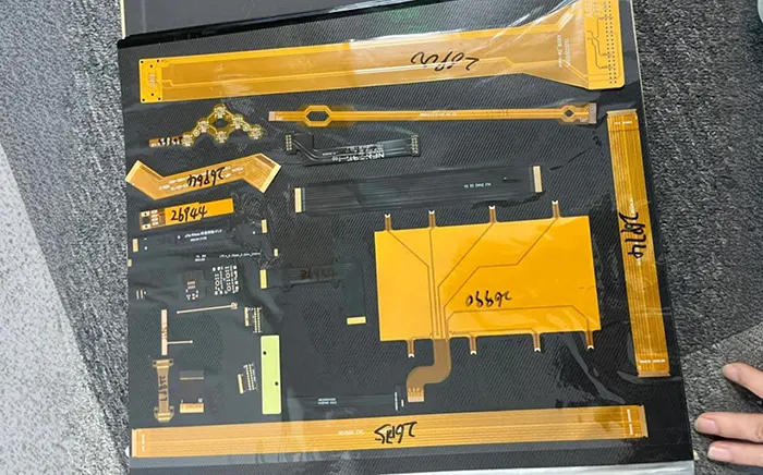
Fpcb
2. Why Engineers Choose Flex PCBs (And Why That Thinking Can Be Dangerous)
Flex PCBs are selected for very rational engineering reasons. The problem is not the intent—it is the incomplete evaluation of system-level constraints.
2.1 The usual motivations
In modern compact electronics design, Flex PCBs are typically chosen for four primary advantages:
| Motivation | Engineering Value | Typical Application |
|---|---|---|
| Space saving | Enables high-density 3D routing | Smartphones, cameras |
| Cable elimination | Reduces connectors and wiring harnesses | Foldable devices, drones |
| Weight reduction | Lower mass than wire harness systems | Aerospace, wearables |
| 3D packaging freedom | Allows folding and spatial integration | Medical probes, robotics |
2.2 The hidden assumption problem
While the motivations for adopting Flex PCBs are generally rational, the underlying decision-making process often contains a subtle but consequential oversight.
The Prototyping Illusion of Reliability
Many engineers unconsciously equate “flexibility” with “robustness,” assuming that a circuit capable of bending is inherently more reliable than a rigid interconnect system.
This interpretation is reinforced during prototyping, where Flex PCBs often appear highly resilient because they can be manually folded, routed through tight spaces, and assembled without immediate failure.
The problem is that prototype behavior does not reflect operational reality. In actual products, reliability is not determined by whether a structure survives a one-time bend during assembly, but by how it performs under continuous mechanical loading, thermal cycling, vibration, and long-term environmental exposure.
Real-World Stress Conditions Beyond Design Assumptions
Once deployed, Flex PCBs are subjected to a combination of stress factors that rarely exist in early design validation.
Bending regions are frequently exposed not only to controlled curvature but also to unintended torsion, axial tension, and assembly-induced deformation.
These additional forces create localized strain amplification that is not always captured in initial mechanical models.
At the same time, repeated thermal expansion and contraction introduce fatigue mechanisms at the copper-polyimide interface, gradually weakening the conductive traces even when no visible damage is present.
Electrical performance is also indirectly influenced by these mechanical effects. Under strain, subtle variations in trace geometry and dielectric spacing can lead to impedance drift, especially in high-speed digital or RF designs.
These changes are often intermittent and difficult to detect during standard functional testing, which contributes to the perception that the system is stable until field failures emerge.
The Non-Linear Relationship Between Flexibility and Reliability
The fundamental issue is that the relationship between flexibility and reliability is not linear.
Flexibility only contributes to reliability when mechanical deformation remains within a tightly defined and carefully controlled operating envelope. Outside of that envelope, the same property becomes a source of stress concentration and fatigue acceleration.
Empirical reliability data from industry and aerospace applications consistently show that Flex PCB failures are more frequently associated with mechanical over-stress conditions and design misapplication than with material defects.
The limiting factor is rarely the intrinsic capability of the flex material system; instead, it is the mismatch between assumed operating conditions and real-world mechanical environments.

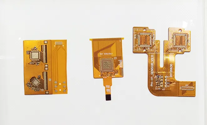
FPCB
The Need for Explicit Mechanical Design Boundaries
This makes Flex PCB design fundamentally different from conventional rigid PCB design.
It requires an explicit definition of mechanical boundaries, including allowable bend radius, expected motion profile, and strain distribution across the circuit stack-up.
Without these constraints being rigorously defined and validated, the perceived advantages of flexibility can quickly transform into latent failure mechanisms that only surface after product deployment.
Flex PCB performance is not governed by flexibility alone, but by a coupled system of:
- Mechanical fatigue behavior (bending radius, cyclic strain)
- Thermal expansion mismatch (CTE interaction with rigid sections)
- Electrical integrity (impedance stability under deformation)
- Material aging (polyimide degradation, copper crack propagation)
Industry reliability data shows that a large portion of flex circuit failures are not due to manufacturing defects, but due to mechanical over-stress outside intended bending design conditions.
In other words, Flex PCBs often fail not in production—but in application.
3. The Core Misconception: Flexibility Is Not Mechanical Strength
A critical engineering misunderstanding is treating “flexibility” as equivalent to “durability.” In reality, Flex PCBs are precision mechanical systems designed for controlled deformation, not general-purpose elastic structures.
A properly designed Flex PCB is optimized for:
- Defined bending radius
- Controlled dynamic flex cycles
- Stable strain distribution within copper foil limits
It is not designed for:
- Random twisting
- Multiaxial uncontrolled bending
- Localized stress concentration (sharp folds, kinks)
- Repeated assembly-induced deformation
Controlled bending vs accidental stress
The distinction can be summarized as follows:
| Parameter | Designed Flex Operation | Real-World Misuse Scenario |
|---|---|---|
| Bending type | Single-axis, defined radius | Random multi-axis deformation |
| Strain distribution | Uniform across bend zone | Localized strain peaks |
| Cycle behavior | Predictable fatigue life | Uncontrolled micro-crack growth |
| Mechanical intent | Engineered motion path | Assembly-induced stress |
IPC reliability research on flex circuits shows that copper traces typically begin fatigue cracking when strain exceeds ~0.3–0.5% under repeated cycling, depending on material stack-up and bend radius conditions (IPC-2223 and associated industry fatigue studies).
Why this misconception persists
The misconception persists because “flexibility” is visually intuitive but mechanically misleading.
Engineers and product designers often observe:
- A Flex PCB can be bent by hand
- It survives initial assembly
- It appears more robust than rigid wiring
But what is not visible is the internal mechanism:
- Copper foil fatigue accumulation
- Adhesive layer micro-delamination
- Stress concentration at via transitions
- Polyimide creep under thermal cycling
These failure modes are slow, cumulative, and often only appear after field deployment.
4. When Flex PCB Becomes the Wrong Choice (Main Technical Section)
Flex PCBs are often positioned as a universal solution for space-constrained and mechanically complex systems.
However, in practice, their advantages are highly conditional. Once design requirements move beyond controlled bending and lightweight interconnects, Flex PCBs can introduce structural and economic disadvantages that are not immediately obvious during early design phases.
The following conditions represent the most common scenarios where Flex PCB adoption becomes technically questionable.
4.1 When bulky components or connectors are required
Flex circuits perform best when the entire system is lightweight, low-profile, and mechanically uniform.
Problems begin when heavy components or rigid connectors are mounted on or near flexible regions.
In such cases, the mechanical mismatch between stiff components and flexible substrates creates localized stress concentration. The rigid-flex transition area becomes a mechanical lever point, amplifying strain during handling, vibration, or assembly.
Over time, this stress concentration typically manifests as delamination between copper layers and the polyimide substrate, or as micro-cracking in copper traces near solder joints.
The issue is not the flex material itself, but the abrupt stiffness gradient introduced by heavy attachments.
A simplified comparison highlights the risk:
| Configuration | Mechanical Behavior | Risk Level |
|---|---|---|
| Pure flex circuit | Distributed stress | Low |
| Flex with small components | Moderate stress variation | Medium |
| Flex with heavy connectors | High stress concentration | High |
In these scenarios, a rigid PCB with external cabling or a hybrid architecture often provides a more stable mechanical platform, particularly when connectors must withstand repeated mating cycles or external force loads.
4.2 When mechanical shock and vibration are uncontrolled
A common misunderstanding is treating vibration as a form of gentle bending. In reality, vibration is a high-frequency fatigue loading condition that repeatedly applies micro-strain to interconnect structures.
Unlike controlled bending, vibration introduces multi-directional stress with unpredictable amplitude and frequency.
This leads to progressive fatigue damage, especially at geometrical discontinuities such as bends, vias, and stiffener boundaries.
Typical failure mechanisms include micro-crack initiation in copper traces and pad lifting at transition zones where rigid and flexible sections meet. These failures are often cumulative and may not be visible until late-stage field operation.
Industries with elevated risk include automotive engine compartments, industrial machinery with continuous vibration sources, and aerospace systems exposed to structural resonance environments.
In these applications, even small design deviations in strain distribution can significantly reduce fatigue life.
4.3 When high temperatures or harsh environments exist
Flex PCBs rely heavily on polymer-based substrates and adhesive systems, most commonly polyimide films and acrylic or epoxy-based bonding layers.
While these materials perform well under moderate thermal conditions, their long-term stability decreases under repeated thermal cycling or elevated temperature exposure.
At elevated temperatures, adhesive layers can begin to soften or degrade, reducing interlayer adhesion strength.
When combined with thermal cycling, the repeated expansion and contraction of copper and polymer layers introduces interfacial fatigue, which can eventually lead to delamination.
Chemical exposure further accelerates degradation. Certain industrial solvents, cleaning agents, or humidity-rich environments can penetrate protective coatings and weaken adhesive interfaces.
A key engineering reality emerges here:
Flex PCB materials are optimized for geometry and packaging efficiency, not extreme environmental durability.
4.4 When high power or heat dissipation is required
Flex circuits are inherently limited by their thin copper structures and low thermal mass. While this is acceptable for signal routing and low-power interconnects, it becomes a constraint in power delivery applications.
The reduced copper thickness restricts current-carrying capacity, increasing resistive heating in narrow traces.
Unlike rigid PCBs, flex circuits have limited ability to spread or dissipate heat across a large thermal plane, which leads to localized temperature accumulation.
Over time, this thermal stress can cause insulation breakdown, material aging, and gradual electrical parameter drift. In high-current applications, the risk is not immediate failure but long-term degradation that reduces system reliability margins.
4.5 When cost sensitivity is critical
Although Flex PCBs are often justified by space savings, their total system cost is frequently underestimated. Unlike rigid PCBs, flex designs require tighter process control, more complex stack-ups, and stricter manufacturing tolerances.
Yield rates are also typically lower due to sensitivity to handling, lamination defects, and material stress during fabrication. These factors contribute to a significant cost differential.
| Cost Factor | Flex PCB Impact |
|---|---|
| Material cost | Higher (polyimide, specialty laminates) |
| Manufacturing complexity | Higher |
| Yield rate | Lower |
| Assembly handling | More sensitive |
In many production environments, the total cost of a Flex PCB solution can be 30–50% higher than an equivalent rigid PCB design, especially when volume scaling is considered. This cost gap becomes more pronounced when mechanical reinforcement or hybrid rigid sections are required.
4.6 When repairability or iteration is required
Flex PCB systems are structurally integrated assemblies. While this improves packaging efficiency, it significantly reduces serviceability.
Once a failure occurs—whether due to trace fatigue, connector damage, or delamination—the repair process is often impractical.
Unlike rigid boards, where components can be replaced or reworked, flex assemblies frequently require full replacement due to their laminated and integrated structure.
This limitation makes Flex PCBs unsuitable for:
- Prototyping-heavy development cycles
- Field-repairable industrial systems
- Modular product architectures requiring frequent upgrades
In these cases, design flexibility at the system level is more valuable than mechanical flexibility at the circuit level.
5. The “Hidden Design Failure Zone” (Unique Insight Section)
One of the least discussed but most critical aspects of Flex PCB reliability lies not in the flexible region itself, but in the transition zones between rigid and flexible sections.
These interfaces concentrate mechanical stress due to abrupt changes in stiffness.
Even when the flex region is properly designed, the boundary areas often experience localized strain amplification that exceeds material fatigue limits over time.
Common stress concentration points include vias located near bend initiation areas, mismatched stiffener boundaries, and copper discontinuities where routing transitions between rigid and flexible zones.
These areas behave as mechanical “weak links” in an otherwise well-designed system.
A key observation from failure analysis across multiple industries is:
Most flex PCB failures don’t happen in the flex area—they happen at the boundaries.
This insight is particularly important because design validation often focuses on the bending region itself, while underestimating the mechanical behavior of adjacent rigid interfaces.
6. Real-World Failure Scenarios (High Engagement Section)
In consumer electronics, repeated folding in devices such as foldable phones often leads to fatigue accumulation in hinge-adjacent flex circuits.
Even when initial testing passes, long-term cyclic folding can initiate micro-cracks that gradually propagate until signal discontinuity occurs.
In automotive environments, Flex PCBs exposed to engine vibration zones frequently suffer from micro-crack formation in copper traces and intermittent electrical failures.
These issues are often difficult to diagnose because they appear only under specific vibration frequencies or temperature conditions.
Medical devices present a different challenge. Sterilization cycles combined with thermal expansion and contraction introduce cumulative material stress.
Over time, adhesive degradation and interlayer separation can compromise signal integrity in critical monitoring systems.
Industrial sensor systems often experience a different failure mode altogether: connector overload.
When flex circuits are used to bridge rigid mechanical housings, external connector stress is transferred directly into the flexible substrate, accelerating failure at attachment points.
7. When Flex PCB Is the Right Choice (Balanced Perspective Section)
Despite the limitations discussed, Flex PCBs remain a highly effective solution when applied within their intended design domain. The key issue is not the technology itself, but the mismatch between use case and mechanical assumptions.
In well-defined engineering environments, Flex PCBs deliver clear advantages. They are particularly effective in systems where geometry is constrained but mechanical behavior is predictable.
This includes tightly packed 3D electronic assemblies where routing space is limited and traditional rigid boards cannot be physically accommodated. In such cases, flex circuits enable interconnect paths that would otherwise require additional connectors or complex wiring harnesses.
Another ideal application is controlled bending systems. When the bending radius, motion path, and cycle count are all defined during the design phase, Flex PCBs can achieve very high reliability.
Wearable electronics are a strong example, especially when deformation is slow, repetitive, and within a known ergonomic envelope rather than random mechanical stress.
Lightweight systems also benefit significantly. In applications where mass reduction is critical, such as portable devices or compact sensing modules, eliminating connectors and wiring harnesses reduces both weight and potential failure points.
Similarly, space-constrained signal routing—particularly in folded or stacked architectures—remains one of the strongest use cases for flexible interconnects.
The engineering conclusion is straightforward:
Flex PCBs are highly effective, but only inside their designed mechanical envelope.
Outside of that envelope, their advantages diminish rapidly and can even reverse into reliability risks.
8. Better Alternatives When Flex PCB Is Not Suitable
When application requirements exceed the mechanical or environmental limits of Flex PCBs, alternative architectures often provide higher reliability and better lifecycle performance.
8.1 Fully rigid PCB + wiring harness
In systems requiring high mechanical robustness or high power transmission, a rigid PCB combined with a structured wiring harness is often the most stable solution.
This architecture isolates mechanical stress from the PCB itself, allowing connectors and cables to absorb vibration and movement.
From a reliability standpoint, this separation reduces stress concentration on solder joints and eliminates the fatigue-sensitive copper flex regions.
It is especially effective in industrial and power electronics systems where mechanical loads are unpredictable.
8.2 Modular rigid + flex cable architecture
A modular approach divides the system into functional rigid PCB units connected by short flex cables or controlled interconnects. This hybrid architecture balances flexibility and maintainability.
Unlike fully integrated flex designs, modular systems allow individual sections to be replaced or upgraded independently.
This significantly improves serviceability and reduces downtime in field applications. It also limits flex exposure to only the necessary interconnect regions, reducing fatigue risk.
8.3 Reinforced hybrid PCB designs
Hybrid rigid-flex structures introduce stiffeners and controlled transition zones to manage mechanical stress distribution. These designs intentionally define where flexibility is allowed and where rigidity must be enforced.
By using mechanical reinforcement layers, engineers can stabilize connector areas and reduce strain gradients at critical interfaces.
This approach is commonly used in aerospace, medical, and high-reliability industrial systems where both compactness and mechanical predictability are required.
8.4 Connector-based separation strategy
In some cases, the most reliable architecture is not integration but separation. By using robust connectors and eliminating continuous flex structures, mechanical stress is localized at well-defined, replaceable interfaces.
Although this approach may increase assembly size, it significantly improves durability and simplifies maintenance. It also allows independent testing and replacement of subsystems, which is critical in mission-critical or long-life industrial equipment.
9. Engineering Decision Framework (High-Value Section for Traffic)
Selecting between Flex PCB and alternative architectures should not be based on intuition or space constraints alone. A structured evaluation of operating conditions is necessary to avoid latent reliability failures.
A practical decision framework can be built around six core questions:
- What is the mechanical load profile? (static, dynamic, vibration, shock)
- What is the thermal environment? (steady-state, cycling, or extreme exposure)
- What are the size and weight of mounted components and connectors?
- What is the required current density or power level?
- Does the system require repairability or modular replacement?
- How strict are the cost constraints across production volume?
These questions define whether Flex PCB is structurally appropriate or inherently overconstrained.
A simplified decision rule can be applied:
If three or more high-risk factors are present—such as vibration, high temperature cycling, heavy connectors, or high power density—then Flex PCB is typically not the optimal architecture.
This does not eliminate Flex PCB as an option, but it strongly indicates that a hybrid or rigid-based system will likely provide better lifecycle reliability and lower total cost of ownership.
10. Conclusion: The Real Engineering Principle
The discussion around Flex PCBs is often framed in terms of technological advancement, as if newer or more flexible automatically means better. In practice, this is not how reliable engineering systems are built.
Flex PCB technology is not a universal upgrade. It is a specialized interconnect architecture designed for specific mechanical and environmental conditions.
When used correctly, it enables compact, elegant, and highly efficient electronic systems.
When used outside its intended envelope, it introduces hidden failure mechanisms that are difficult to detect during early validation.
The broader engineering principle is not about maximizing capability, but about matching constraints to reality.
Every interconnect strategy—whether rigid, flex, hybrid, or modular—has an optimal operating domain. The goal of engineering design is to identify that domain accurately, not to force one technology into all scenarios.
A more precise way to frame the conclusion is this:
The best PCB is not the most flexible one—it is the one least likely to fail in your real environment.
Sources
- IPC-2223: Sectional Design Standard for Flexible Printed Boards
- IPC-6013: Qualification and Performance Specification for Flexible Printed Boards
- NASA GSFC-STD-7000: General Environmental Verification Standard for GSFC Flight Programs
- JEDEC reliability studies on interconnect fatigue and thermal cycling
- MIL-STD-810H: Environmental Engineering Considerations and Laboratory Tests
- IEEE Transactions on Components, Packaging and Manufacturing Technology (flex circuit fatigue and thermal reliability studies)
- Z. Wang et al., “Fatigue behavior of copper traces in flexible printed circuits,” Microelectronics Reliability Journal
- 1. The Hidden Truth About Flex PCBs
- 2. Why Engineers Choose Flex PCBs (And Why That Thinking Can Be Dangerous)
- 3. The Core Misconception: Flexibility Is Not Mechanical Strength
- 4. When Flex PCB Becomes the Wrong Choice (Main Technical Section)
- 5. The “Hidden Design Failure Zone” (Unique Insight Section)
- 6. Real-World Failure Scenarios (High Engagement Section)
- 7. When Flex PCB Is the Right Choice (Balanced Perspective Section)
- 8. Better Alternatives When Flex PCB Is Not Suitable
- 9. Engineering Decision Framework (High-Value Section for Traffic)
- 10. Conclusion: The Real Engineering Principle
- Sources

