
High-Frequency Rigid-Flex PCB Manufacturing: Key Process Technologies Using PTFE Materials
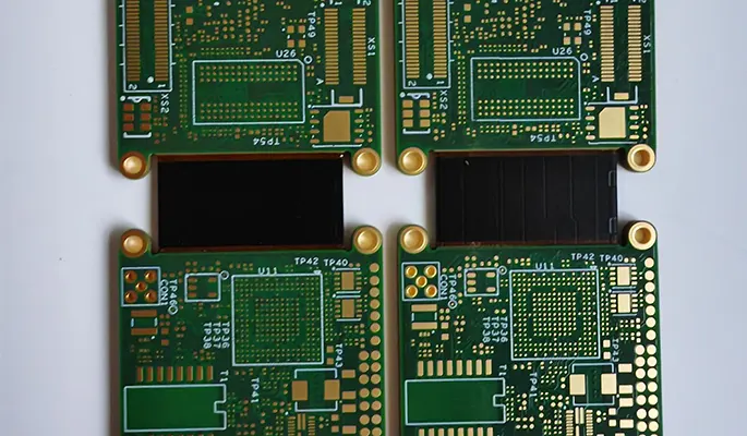
High-frequency rigid-flex PCB manufacturing combines rigid board stability with flex circuit movement, and it often relies on PTFE materials for low signal loss. In this 10-layer rigid-flex manufacturing example, the flexible zones run from L2 to L9, so eight of the ten layers serve as flex layers. Both the flexible-zone substrate and the pure adhesive bonding sheets (BS) are PTFE-based high-frequency materials, and because the substrate is customer-supplied, the fabricator works from a fixed material set for this PTFE high-frequency rigid-flex build. The article follows that build through its key process technologies: base material testing, lamination, drilling, plasma treatment, and impedance control.
Key Design Specifications
Design item and technical requirement are summarized below.
| Design Item | Technical Requirement |
|---|---|
| Material (BS) | FR-**Z |
| Number of Flex Layers | 8 L |
| Total Layer Count | 10 L |
| Finished Board Thickness | 1.7 ± 0.075 mm |
| Minimum Hole Diameter | 0.2 mm |
| Maximum Aspect Ratio | 8:1 |
| Layer Misalignment | ≤ 0.15 mm |
| Resin Overflow | ≤ 0.5 mm |
| Impedance Tolerance | ±10% |
These values drive every downstream step. For example, the 0.2 mm minimum hole and the 8:1 aspect ratio set the drilling and plating window. Also, the ±10% impedance tolerance defines how tightly lamination and etching must be controlled.
Why PTFE Materials Are Used

High-frequency material spectrum
High-frequency FPC work currently uses MPI, LCP, and PTFE. Among them, PTFE shows the lowest loss factor, with Df < 0.002 @ 10 GHz. As a result, it meets insertion loss testing requirements for higher frequencies.
PTFE Rigid-Flex Manufacturing: Base Material Testing Comes First
PTFE rigid-flex manufacturing starts with incoming material testing. The substrate here uses a PTFE resin system, and suppliers describe its behaviour in different ways.
For example, Company R states its PTFE material shows no significant self-healing over time, while Company S reports a different result. Therefore, the process team checks each material before release.
Points to Confirm in Material Testing
- Loss factor and insertion loss performance at the target frequency.
- Self-healing behaviour reported by each supplier.
- Resin overflow, kept at or below 0.5 mm.
- Layer misalignment, kept at or below 0.15 mm.
Lamination and Drilling in 10-Layer High-Frequency Rigid-Flex Builds

Product Stacking Information Diagram
Product Process Flow:
Cutting → Drilling → Inner Layer Pattern 1 → Inner Layer Etching 1 → Inner Layer AOI 1 → Brown Coating → Lamination 1 → Drilling → Plasma → Electroplating Copper → Electroplating → Inner Layer Pattern 2 → Inner Layer Etching 2 → Inner Layer AOI 2 → Cover Film Lamination → Brown Coating (Completion of Flexible Area) → Laminate 2 → Drilling → Plasma → Electrolytic Copper Plating → Electroplating → Outer Layer Pattern → Outer Layer Etching → Outer Layer AOI → Solder Mask → Controlled Depth Milling → Cover Removal → Gold Plating → Characterization → Forming → Electrical Testing → OSP → FQC → FQA → Shipping
The board passes through two lamination cycles. First, lamination 1 bonds the inner stack after brown coating. Next, laminate 2 joins the outer layers once the flexible area is complete.
Drilling appears three times in the flow: after cutting, after lamination 1, and after laminate 2. Because the finished thickness is 1.7 ± 0.075 mm, hole quality and registration must hold through every cycle.
Plasma Treatment and Copper Plating
Plasma treatment follows drilling and comes before copper plating. It prepares the hole walls and the PTFE surfaces so plating can bond reliably. Then electrolytic copper plating and electroplating build the conductive layer.
Additionally, the flexible area needs its own protection. Cover film lamination and brown coating complete that zone before the second lamination.
Impedance Control and Surface Finish
Impedance tolerance stays within ±10% across the board. However, that target depends on stable dielectric thickness and consistent etching.
The final steps include solder mask, controlled depth milling, and cover removal. After that, gold plating, characterization, and forming prepare the panel. Also, electrical testing, OSP, FQC, and FQA close out the build before shipping.
Full Process Flow for the 10-Layer High-Frequency Rigid-Flex Board
1. Cutting, drilling, inner layer pattern 1, inner layer etching 1, inner layer AOI 1
2. Brown coating, lamination 1, drilling, plasma, electroplating copper, electroplating
3. Inner layer pattern 2, inner layer etching 2, inner layer AOI 2
4. Cover film lamination, brown coating (completion of flexible area), laminate 2
5. Drilling, plasma, electrolytic copper plating, electroplating
6. Outer layer pattern, outer layer etching, outer layer AOI
7. Solder mask, controlled depth milling, cover removal
8. Gold plating, characterization, forming, electrical testing
9. OSP, FQC, FQA, shipping
FAQ
What is a 10-layer high-frequency rigid-flex PCB?
A 10-layer high-frequency rigid-flex PCB is a ten-layer board with flexible zones, here from L2 to L9. Its flexible substrate and pure adhesive bonding sheets use PTFE-based high-frequency materials. Typical specs include a 1.7 ± 0.075 mm finished thickness, a 0.2 mm minimum hole, an 8:1 maximum aspect ratio, and ±10% impedance tolerance.
Why does PTFE rigid-flex manufacturing need base material testing?
PTFE rigid-flex manufacturing needs material testing because suppliers describe PTFE behaviour differently. For example, Company R reports no significant self-healing over time, while Company S reports a different result. Testing also confirms loss factor, with PTFE reaching Df < 0.002 @ 10 GHz, so insertion loss stays within limits.
Which process steps matter most for a 10-layer high-frequency rigid-flex board?
Material testing, lamination, drilling, and plasma treatment matter most. Two lamination cycles bond the stack, three drilling steps hold the hole pattern, and plasma treatment prepares the holes before copper plating. Together, they keep layer misalignment at or below 0.15 mm and impedance within ±10%.
Related Posts
- High Frequency Flexible PCB Impedance Control Guide — Related article
- High-Frequency High-Speed FPC Materials for 6G Part I — Related article
- High-frequency FPC materials: LCP, MPI & Low Loss Guide — Related article
- PTFE Blind Via Metallization for High-Frequency FPC — Related article
- Rigid-Flex PCB Air-Gap Process Optimization for High Yield — Related article